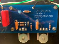
Compare the two boards visually for differences, both on boards and wiring.
Just triple checked and the boards are stuffed identically, with all components in their correct places and orientations, and the board is getting + and - voltages properly from the PSU, as the LEDs are lit.
Across what components should I start checking voltages?
Please post a photo of your board, in case others can spot something you missed.
Perhaps start with a few basic measurements:
What's your DC offset?
What voltages do you see across D1, R7-R8, R16-R19. (Also please identify what you are using for R7 and R8)
Perhaps start with a few basic measurements:
What's your DC offset?
What voltages do you see across D1, R7-R8, R16-R19. (Also please identify what you are using for R7 and R8)
Please post a photo of your board, in case others can spot something you missed.
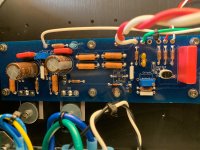
Here are two shots (left and right sides of the same board) of the channel that's not working. The opposite channel is working perfectly and shows zero DC offset at 400mv of bias. I will make your suggested measurements later today and get back to you with the results.
Thank you.
Attachments
I .had this same issue. PS wasn't connected to the non working side properly.
How's the Q's orientation?
How's the Q's orientation?
@bpr - Once you post some measurements, it'll be easier to nail down. Regardless of root cause determined, perhaps show a little more love to Q5. If you've soldered it from the top side, the joint on the gate may be a little sketchy long-term. I don't see anything that jumps out re: stuffing, but perhaps other eagle-eyed observers will notice something.
Nice photos. Easy for bad eyes to zoom in 🙂
Edited to add - Maybe a reflow for the gates of Q6 and Q8 too, since the iron's hot.
Nice photos. Easy for bad eyes to zoom in 🙂
Edited to add - Maybe a reflow for the gates of Q6 and Q8 too, since the iron's hot.
Last edited:
What's your DC offset?
What voltages do you see across D1, R7-R8, R16-R19.
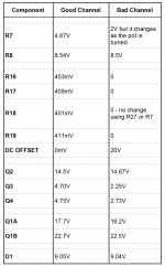
Here's what I got when measuring, per your recommendation:
D1: -9.09V
R7 (pot): Fluctuated between -790mV and -1.1V
R8 (1k ohm): -8.5V
R16 - R19: Nada - no voltage across any of these. R18 on the working channel of the amp is still between 400mV and 410mV. I didn't test the R16, 17 and 19 on the good side, but assume they're doing what they're supposed to.
How's the Q's orientation?
All good. Checked a fourth time just to make sure.
perhaps show a little more love to Q5.
Maybe a reflow for the gates of Q6 and Q8 too, since the iron's hot.
I will reflow those Qs once I figure this out - thanks for the heads up.
The voltage across R7 is problematic. It should be 4.x volts or so.
Does it go up if you try adjusting R7?
Please verify that the jfets are well soldered.
Does it go up if you try adjusting R7?
Please verify that the jfets are well soldered.
Does the voltage across R7 change when you adjust the pot? It should't fluctuate just sitting idle.
Edited to add - That'll teach me to refresh before posting. Listen to Dennis. 😀
Edited to add - That'll teach me to refresh before posting. Listen to Dennis. 😀
Does it go up if you try adjusting R7?
Please verify that the jfets are well soldered.
The voltage at R7 does go up or down when the pot is turned one or the other way, yes. And the jfets seems as well soldered as they do on the working channel.
Does the voltage across R7 change when you adjust the pot? It should't fluctuate just sitting idle.
I made a lazy voltage test the last time. I fixed my method and the voltage doesn't fluctuate more than a couple millivolts when the pot it static. Voltage changes as pot is turned.
Does it go up if you try adjusting R7?
Does the voltage across R7 change when you adjust the pot?
Help me make sure I'm measuring R7 properly. In the attached photo, I'm measuring the voltage drop across the pot at these two points (circled in green) on the board. Is this correct?
Attachments
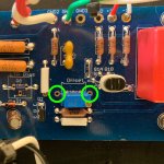
For measuring across R7, that is correct.
BTW, lots of internet points awarded for positioning the resistors in a manner that makes them easy to read. We collectively thank you.
Also, connect -IN to GND. (Unless you are feeding it via XLR)
BTW, lots of internet points awarded for positioning the resistors in a manner that makes them easy to read. We collectively thank you.
Also, connect -IN to GND. (Unless you are feeding it via XLR)
BTW, lots of internet points awarded for positioning the resistors in a manner that makes them easy to read. We collectively thank you.
Also, connect -IN to GND.
Awwww. Yer makin' me blush... but you are welcome. It's bad enough if I can't read values on the resistors, but another thing entirely when you're asking for help from strangers, and they can't read them. I just appreciate the guidance.
And to check, connecting -IN to GND is connecting the circled pads in the attached photo, yes?
Attachments
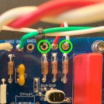
Yes, that is the place for the jumper. Note, as 6L6 mentioned, you do not need the jumper if you are planning to wire only XLR inputs or both XLR and RCA. Then, you can choose to either have pin 1 from the XLR run to that point or to the chassis. That decision is yours, but there are strong well-founded opinions/reasons that Pin 1 should go to the chassis. If that was already your plan, then 🙂
Excellent that the voltage at R7 is stable at a given pot setting. What is your offset on the "bad" channel as-is? Does it vary when you turn R7? It should given your measurement, but I didn't see that earlier. Noted that you have 0V across R16-R18.
Does the voltage at R18 vary when you turn R27a (bias pot)?
If no, provide measurements like in post #5766. I like the brandy suggestion. 🙂 It may be easier to take them all at once rather than measure, post, measure, post. No need to post measurements from the good channel.
Trying to not have too many people provide guidance. If 6L6 and Dennis are on the case, you're in excellent hands.
Last edited:
I'd been looking for that post, as I'd remembered reading it. Thanks for finding it. I've attached a list of all measurements of both sides of the amp.If no, provide measurements like in post #5766.
If 6L6 and Dennis are on the case, you're in excellent hands.
I'm in good hands with all three of you. Thanks again for taking the time to help.
Attachments
@BPR - I've stared at this a few times and admit that I'm stumped. It will probably be obvious to someone else. I'm sure you'll get a clear path forward soon.
I'd been looking for that post, as I'd remembered reading it. Thanks for finding it. I've attached a list of all measurements of both sides of the amp.
I'm in good hands with all three of you. Thanks again for taking the time to help.
Q2 is properly biased; Zener voltage is okay.
Your output stage is floating at the DC rail voltage (hence the DC bias sitting at 20V DC) -> because Q7 and Q8 are not conducting the current. They are not conducting the current because the voltage drop across R7 must be 4.3V to "open" the Q7 and Q8 MOSFETs.
The voltage drop across R7 is not sufficient enough, because there is not enough current running through Q1A JFET (or, there is enough current, but it is routed via a different, undesired path...):
1. (most likely) the Q1A and Q1B are faulty. Replace them. While at it, replace the Q2 just in case (very cheap, just cut the legs and then remove one leg at the time with tweezers)
2. There is a large current draw, from Q1A through R11 and/or R12 via faulty MOSFET's Q7 and Q8. So, a) Check the MOSFETs, and b) Make sure they are electrically isolated from the heatsink.
I'd replace Q1A, Q1B and Q2 first, WHILST at the same time, making sure the Q7 and Q8 are okay AND they are electrically isolated from the heatsink.
Last edited:
I'd replace Q1A, Q1B and Q2 first, WHILST at the same time, making sure the Q7 and Q8 are okay AND they are electrically isolated from the heatsink.
I replaced Q2 and checked that the MOSFETs were all electrically isolated, which they are. I need to order new LSJ74s to replace Q1A and Q1B. If I purchase another matched quad set from the diyAudio Store, will I need to replace Q1 and Q2 on the properly operating side of the amp, so that everything is matched on both sides?
Also, thank you for being so clear in your explanation of what is happening in the circuit. I understood how it worked on a global level, but your efficient and concise description really helped me understand why I'm seeing the issues on the bad channel.
I will report back once I have the new JFETs in hand and installed.
You do not have to worry about the good working side. So, a matched quad will leave you with a matched pair for future builds. I'd use a grounded antistatic wrist strap. Once the JFETs are soldered, you can remove the strap.
There is a large current draw, from Q1A through R11 and/or R12 via faulty MOSFET's Q7 and Q8. So, a) Check the MOSFETs
I should have asked this on the last post, but is there a way to check if Q7 and Q8 are working properly, without de-soldering them from the board?
- Home
- Amplifiers
- Pass Labs
- Aleph J illustrated build guide