they are available at digikey. If not available in ukraine let me know and I can send them to you. I am about to order some for me!replace SST404
I prefer to cut the leads at the point where they connect to the body of the transistor, then remove each lead frommthe PCB with an iron and tweezers. Then I remove excess solder from the pads using solderwick.Please tell me how you can replace SST404? Thank you.
Finally, scrub with a cottonbud soaked in isopropyl alcohol, then put a new SST404 on.

JFE2140 is quite similar and seems to work in sims. Pinout is different though.The SST404 is pretty fundamental to the design.
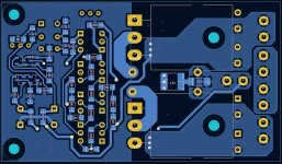
I was thinking of using the JFE2140 as well. Also, its layout is identical to the LSK389 series, so there would be options for trying those as well. Entirely possible the source resistors might need to be tweaked as well as the current and maybe the compensation. As Suzy was kind enough to provide the Kicad files I though it would just be a small change. But one change led to another and "why not change this" so my layout has moved a bit from the original. I just ordered boards so the etch has not been validated but I would be happy to share if there is interest.
I added bulk caps to the +/- rails. This stretched the board by 12mm. Width is unchanged.
Attachments

Last edited:
As I noted, one change led to another, as is often the case. I decided to increase the spacing between the rows of T0-126 transistors such that a heatsink would be made from 0.125" bar stock. While cleaning up the mess that made I noticed the gate drive traces were quite different in length. I decided to swap the output transistor locations which made the gate drive traces almost equal. Also note that the ground area under the ouput devices is no longer split by the feedback trace. I believe I have properly considered where high currents flow and connected "earth" to a quiet location.
With all these changes I didn't think it appropriate to keep the Suzy logo, but want to pay tribute to her original work, hence the name Myka-SJ. Myka is my hardware design consultant...
With all these changes I didn't think it appropriate to keep the Suzy logo, but want to pay tribute to her original work, hence the name Myka-SJ. Myka is my hardware design consultant...
Very cool. This sort of thing us exactly my intent in publishing the KiCad files.
I have stuffed and powered up a board of my layout. Two small erata on the silkscreen. The Cathode mark on ZD4 was missing as were the reference designators for Q19 and Q21. Bringing the board up it wanted to oscillate so I changed C3 to 100pF and that allowed the full rail voltage to be applied. No idea yet if that is an optimal solution but an LTSpice simulation is good with it. I also changed R15 and R16 to 20 ohms from the zero ohm value. I have attached the Kicad archive file.
Attachments
A construction issue that I was vaguely aware of but did not specifically address during layout is that the clamping force for the output devices includes the PCB in the stack-up if the top surface of the device rests directly against the PCB. This would violate design rules for any of the companies I worked for because the PCB material itself is understood to “cold-flow” and over time the clamping pressure is reduced.
Given that the PCB uses the output device mounting to support the board I think the easiest solution is to use a thru hole in the heatsink and after passing a screw through the heatsink and the device, secure the device with a flat washer, locknut and a threaded standoff. Using a ¼” standoff would allow a ½” standoff to be used with the two mounting hole locations included on the PCB.
There are of course a number of other options, including choosing to ignore the issue. But after years of beating young engineers with a stick for violating design rules ...
JA this may be better in a separate thread, but you could start with the offset adjust to see if it makes a difference. Likely to input fet or close by. Interestingly I remember from back in the day a number of people could not get DC stability with this design and resorted to servo's. Maybe they didn't use close match parts but it was a "thing".
Yes, thanks Triplej I'll trim the offset as soon as I get some time.
Although the very sudden drift sounds more like a component failure.
Although the very sudden drift sounds more like a component failure.
- Home
- Amplifiers
- Solid State
- AEM6000 Based 50W Amp