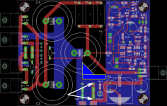
That +Vout connector blade (white arrows) cuts a big slot in the blue plane, perpendicular to the direction of current flow. Undesirable.
Why not add some more blue, above the slot, giving more of an unimpeded pathway from the Gnd connector blade, to the remainder of the blue plane? And also from the filter cap ground point, to the remainder of the blue plane.
Suggest adding triangle and rectangle.
_
Why not add some more blue, above the slot, giving more of an unimpeded pathway from the Gnd connector blade, to the remainder of the blue plane? And also from the filter cap ground point, to the remainder of the blue plane.
Suggest adding triangle and rectangle.
_
Attachments
or ensure the return route can mimic the flow route for that current by placing the plane over/under the trace that carries the flow current.
It's all about reducing LOOP AREAS.
It's all about reducing LOOP AREAS.
Ok thanks a lot guys. Revised version attached (plus an image highlighting the bottom layer ground plane with the top layer turned off). To Andrew's point, I could easily extend the plane to include the area marked in lime green. This would run GND under the main top layer trace to the pass transistor. (Similarly, I could expand it to include the trace powering all the regulator components driving the gate.) However, I also understood that there is a desire to 'isolate' the pulses flowing from the rectifer caps and hence we take a definitive 'spur' from this junction area where C3-C5 meet. It was this thinking which drove the shape of my earlier draft (although I see the problem it presented.) (Rightly or wrongly I visualise this as ping pong balls bouncing off the edges of this GND area. slowly reducing velocity and one wanting to reduce the chances that a pulse directly slots down spur.🙂)
On another note, I was unaware of the LM336-2.5. Instead I have provided for the use of LM4040-2.5 as the voltage references for the 5V and 3V3 rails. I guess I could have saved myself a bit of board area. I have already purchased some of the A version LM4040-2.5. If I should switch to the LM336-2.5 please let me know. I used LM4040A-5 (vs LM329) for Z2 largely because of its availability in SOT-23 pakage.
On another note, I was unaware of the LM336-2.5. Instead I have provided for the use of LM4040-2.5 as the voltage references for the 5V and 3V3 rails. I guess I could have saved myself a bit of board area. I have already purchased some of the A version LM4040-2.5. If I should switch to the LM336-2.5 please let me know. I used LM4040A-5 (vs LM329) for Z2 largely because of its availability in SOT-23 pakage.
Attachments

... I have already purchased some of the A version LM4040-2.5. If I should switch to the LM336-2.5 please let me know ...
Please ask your circuit designer to write up her comparative analysis, '336 vs '4040 , and post it here. I imagine there is a ~ 60% probability that I will wind up agreeing with its conclusions.
In favour of LM4040 A series:
1. far tighter output voltage tolerance (0.1% versus 1% or 2% although now I see there is also the LT1009 which has a 0.2% initial tolerance)
2. much smaller package
3. I own them (albeit this is a minor consideration)
Disadvantages
3. worse noise by some magnitude
4. LM336 has same package as LM329 and so no need for two board placeholders for Vref
I'm unsure how to weigh 1 vs 3 although the LT1009 would seem to level the playing field re 1 and tilt me in favour of the LT1009.
Your load is a digital circuit whose power supply tolerance is 10%. I suggest you make the choice based on output impedance (since lower Zout gives higher input ripple rejection in a Sulzer-style regulator which biases the VREF from the ripply input), noise, and packaging convenience. I think the LT1009 might rank highest, followed by 4040, followed by 336.
Thanks. I looked at "reference impedance" and, in the case of the LM4040, "reverse dynamic impedance". There didn't seem to be much between them. Perhaps I misread the sheets. In any event I will change to the LT1009 for the 5/3.3V refs. For the level shift on the 12V I currently have a LM4040-5V. Again I am wondering if the lower noise of the LM329 wouldn't be better particularly given the outright level of shift isn't important.
Let's suppose your load draws 0 to 5A. Since it is a computer, load current is going to be rather chaotic. Even with a very good output impedance in the 1 mOhm range, this means the output voltage is going to fluctuate 5 mV at least.
If you got 100µV noise/ripple on top of that, who cares.
I suggest you don't worry too much about noise. You could use a TL431 as a reference. Also your expensive AD797 might be overkill...
IMO for this type of reg and load, you don't really need to think too much about noise, what matters is transient response (ie, absence of undershoot, overshoot, or damped oscillations at all load currents, when connected to the target load and its onboard capacitors).
You are right that I need to keep a sense of perspective. I do think, however, this reg circuit could have quite a lot of potential for a lot of lower current applications (and even better in such case if I can figure out thermal considerations for a pass transistor such as the BUK9K35-60E).
Speaking of the TL431, I keep forgetting I have a few Exar SPX431 - an improved version of the TL431 - and that if I leave Vref unconnected it's a 2.5V reference. Duh. (My adventures started with the idea of using the SPX431 to drive the adjust pin of an LT1084 (in the same way that the TL431 can be used with an LM317). That exploration hit serious doubts.)
I think I am right in saying that using the SPX431 here as a simple shunt voltage reference doesn't involve the same nested feedback risks I was encountering in that earlier work so I can make use of parts I already have. Output impedance is much lower than the LT1009 and noise lower also. Overkill? Probably, but if they are a worthy substitute it beats leaving them lying in the draw and purchasing a lesser part.
For fast changing currents, as in most digital circuits, the current demand changes are met by the HF local decoupling capacitors. One on just about every power pin.
These are recharged by the nearly local MF decoupling electrolytics. Dozens to hundreds of 1uF to 22uF spread around the PCB.
The regulator recharges the MF and HF decoupling capacitors.
These are recharged by the nearly local MF decoupling electrolytics. Dozens to hundreds of 1uF to 22uF spread around the PCB.
The regulator recharges the MF and HF decoupling capacitors.
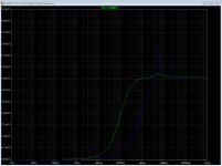
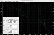
Dude you want a logarithmic scale on the vertical axis so you can see exactly what "close to zero ohms" really means.
And aren't you intrigued to run transient analysis when you hang a 1-ampere, 5 MHz sinusoidal current source on the output with 4 amps of DC load flowing? Don't ya want to know whether the blue peak at 5MHz is anything to fear?
And aren't you intrigued to run transient analysis when you hang a 1-ampere, 5 MHz sinusoidal current source on the output with 4 amps of DC load flowing? Don't ya want to know whether the blue peak at 5MHz is anything to fear?
Yeah I just hate scientific notation. Need to get used to it.
I was fearing it. It's not good...it breaks into oscillation when I add on the sinusoidal (SINE(4 1 5Mega 0.2)). I'm trying to rationalise this versus earlier phase and gain margin analysis...🙁
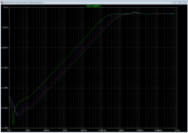
5MHz is where phase passes through -180 degrees (thereabout for all loads). Here I see 11dB plus of gain margin for 5A and more for lighter loads. I'm obviously missing something important re stability and presumably need even more gain margin.
I was fearing it. It's not good...it breaks into oscillation when I add on the sinusoidal (SINE(4 1 5Mega 0.2)). I'm trying to rationalise this versus earlier phase and gain margin analysis...🙁
5MHz is where phase passes through -180 degrees (thereabout for all loads). Here I see 11dB plus of gain margin for 5A and more for lighter loads. I'm obviously missing something important re stability and presumably need even more gain margin.
Last edited:
If this thing has flat impedance below 10 mOhm from 10Meg to 1 GHz, either you get nobel prize, or your spice model has a slight problem. I suggest investigating the second option, which may also explain the peaking...
Square wave load test is also nice (and very easy to do on a real circuit, all you need is a scope and a 74AC14 for those extra crispy 2ns rise time current pulses, it has no mercy for circuits with funky transient response / settling / marginal stability).
Square wave load test is also nice (and very easy to do on a real circuit, all you need is a scope and a 74AC14 for those extra crispy 2ns rise time current pulses, it has no mercy for circuits with funky transient response / settling / marginal stability).
Last edited:
I understood that it was typical/normal for impedance to approach the series resistance of the output caps at high frequencies. (I can't find the exact source where I read this at the moment - likely Cordell.) It's certainly consistent with the output above - two caps in parallel each with 10mR of ESR.
I've spent some time with the models and even more re-reading all of Cordell's pages on negative feedback and stability. The models I have done for phase and gain margin analysis at various loads and transient load changes (extreme square wave step in DC current load) all seem okay. I have swapped out the op amp for an LT1498 in the model and it exhibits the same impedance behaviour.
The output above is with a Zobel network (100p cap in series with a 47R resistor) from drain to gate of the series pass transistor. A similar impedance plot appears with a plain 100R gate stopper resistor. With the Zobel at the gate, the op amp compensation is a simple Miller integrator of 47p. Increasing the size of the Miller capacitor has no affect on the impedance peaking but of course lowers fc and hence higher frequency PSRR. With the gate stopper, the op amp compensation requires a resistor in series with the Miller capacitor - a form of compensation discussed by Cordell also. I re-examined the output capacitors and looked at adding higher ESR there - it worsens gain margin.
I've read a lot about gain peaking being an indication of instability but I'm struggling to find a discussion regarding impedance peaking. I will keep digging but I am feeling way out of my depth here even when I now feel I can follow a good deal of discussion regarding negative feedback stability and amplifier compensation. Perhaps I am missing something even more basic.
I also quickly looked at stepping a sinusoidal current load (i.e. beginning with 4A DC current load and adding the sinusoidal current load after a short delay) of much lower frequency than 5MHz. The problem persists.
I will keep digging...
Indeed I don't have the ESL of the output capacitors in the model because this information isn't available in the data sheet (it's there for the main filter caps). And I have not modelled trace resistance or inductance, nor anything downstream of the output from the regulator (wiring to my TPS3510 power control board, that board itself and wiring from there to the motherboard) - except the test load. Are you suggesting that this wiring resistance and inductance will likely mean the modelled peaking in regulator impedance is a non-issue (in like manner to the issue I had when I slapped on a lump of load capacitance)? This is one of the things I wanted to try tomorrow if I can carve out the time...
C12/C13 should be about 6-8 nH, the big SMT one a little more if you add some vias on its GND pin, or a whole lot more if you don't 😉
Capacitor ESL can make your circuit more stable (or more unstable, depending on Murphy's mood)...
Capacitor ESL can make your circuit more stable (or more unstable, depending on Murphy's mood)...
Ok adding capacitor ESL had an enormous impact on output impedance with the peaking more severe. But it improved phase and gain margin. It did not stop the oscillation with a transient to 1A of sinusoidal (+4A DC) current load. (Neither did adding the resistance and inductance of 15cm of 16AWG wire.)
I'm at a loss. Have I hit yet another dead end?
(Thanks for the tip re bias on the ground pad of the SMD cap. I had a trace linking its ground pin to the ground pin of the nearest through-hole component. I will edit the board to deploy vias on the pad itself.)
I'm at a loss. Have I hit yet another dead end?
(Thanks for the tip re bias on the ground pad of the SMD cap. I had a trace linking its ground pin to the ground pin of the nearest through-hole component. I will edit the board to deploy vias on the pad itself.)
Attachments
- Status
- Not open for further replies.
- Home
- Amplifiers
- Power Supplies
- Adventures with 5A regulated voltage circuits