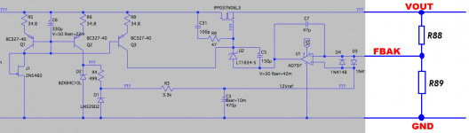
It seems to me that if VOUT is actively pulled down by a load resistor, then resistor R88 holds node FBAK down too.
If node FBAK is held down, then diode D4 holds down node 12Vref too. There is a tug of war between (the load resistor in series with R88), and filtering resistor R3. Node 12Vref cannot rise freely.
This situation persists while the drain of the MOSFET slowly rises. Q3 helps the gate rise too, so the MOSFET acts as a source follower, pulling up VOUT to a voltage equal to Vdrain - Vthreshold. The 5V zener action of U2 ensures that the gate rises up to at least 5 volts, before opamp U1 has any control whatsoever.
Attachments
Thanks Mark. I believe that after witnessing the ramp in Vref I confused the charging of capacitance and the voltage potential of Vref, expecting Vref to rise from zero to 6.9V over 5 time constants even with no load.
In my real circuit, load will be de minimis (only leakage plus 5V used for standby operation) until the Vouts are up to spec. (Only then will the TPS3510 control board convey PWR_OK and open its pass transistors.) So I think I am right in expecting the three rails to come up to spec almost immediately rather than over many seconds. Perhaps I should model a set of switches that connect the load after x milliseconds. (If nothing else it might speed the sim.)
In my real circuit, load will be de minimis (only leakage plus 5V used for standby operation) until the Vouts are up to spec. (Only then will the TPS3510 control board convey PWR_OK and open its pass transistors.) So I think I am right in expecting the three rails to come up to spec almost immediately rather than over many seconds. Perhaps I should model a set of switches that connect the load after x milliseconds. (If nothing else it might speed the sim.)
Last edited:
The above is still bugging me a bit but I think I will just move on. I have a current load for each voltage stepping from zero to 5A but only after an extended period of time (10s). The 12V comes up to 12V almost immediately. With the 5V and 3V3 I have to model the 12V voltage powering the op amps and supplying initial voltage to their Vref zeners and respective low pass filters as a perfect voltage source rather than coming from the 12V rail else the model takes an eternity to run (i.e. I can leave it running overnight and it still won't complete). Even with no load those rails show the asymptopic rise in voltage over a many seconds that I witnessed on the 12V rail when it had a small initial load (while the 12V doesn't with no load). Confused.
While I add the bleeder resistors and make final changes to the board, I noted this thread and the comments about grounding structures. Until now I was planning on just doing a ground plane for the whole board (top and bottom layers). Having read the comments regarding bringing the dirty grounds together before connecting to the rest of the board I am wondering if I shouldn't amend this strategy.
Thoughts? Or are the points made in that thread only relevant for a choke input filter?
Last edited:
Have you read Cordell section 16.9, "Grounding Architectures" ?
Have you read Self chapter 25, "Layout, Grounding, and Cooling" ?
Have you read Self chapter 25, "Layout, Grounding, and Cooling" ?
I had read Cordell some time ago but not Self. I went through them both last night. I will work on the board and try to implement what I understand to be their recommendations. Will revert.
Okay hopefully I am heading in the right direction...
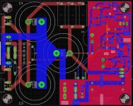
Ground connections for rectifier diodes and main filter caps only on bottom of the board (blue). I understand the goal is for these to be 'resolved locally' (although to be honest I don't follow how this happens when everything is all connected). Should I literally bring, in 'star' fashion, the ground connections for C3-C5 to a central, singular point, perhaps where the connection from D2 would meet i.e. underneath C4, or does the polygon I have drawn do the job better? The polygon is my interpretation of Self's "thick earth connection; this is called Reservoir Ground".
The pink polygon is a ground plane, top and bottom, for everything else. It obviously needs to be connected to the other ground traces. Self mentions with respect to Reservior Ground that one shouldn't "attempt to use any point on this track as the audio-ground star-point, as it carries heavy charging pulses". Now, this entire board is a power supply but I presume it is desirable follow his guidance: "Instead take a thick tee from the centre of this track (through which the charging pulses will not flow) and use the end of this as the star point." It's not clear to me where this tee is best placed. If I had to guess I would bring it across from the top of the 'toe of the (pink) boot'.
Attachments
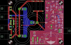
All of the diode-capacitor charging pulses flow in metallic traces to the left of C5's ground terminal. So you could tap off from the right side of C5's ground terminal on the blue layer, route it downward to the red groundplane and take advantage of the (yellow arrow) big thru-the-board connections at the GND QuickConnect blade. You can also use a machine gun to install seven gerbillion vias (white ellipses) between the blue and the red. Moving that LED to the crotch between C3 and D4 might let you create a more robust connection.
By the way the blue traces between D3 & D2, and between D2 & the capacitors, appear needlessly narrow.
By the way the blue traces between D3 & D2, and between D2 & the capacitors, appear needlessly narrow.
Attachments

Load capacitance.
I'm getting unstuck when I add load capacitance to my regulator circuit.
It is not possible to design a regulator without knowing what capacitors are going to be on its output. That includes the C, ESR, ESL and the inductance of the connection between everything. All this is part of the same circuit and should be designed together.
The less you know, the more compromises you gonna have to make (mostly in adding resistance somewhere, real or synthetized with feedback). If you need unconditional stability, you gonna have to make some compromises you're not gonna like. And it's not gonna be really unconditional either...
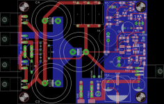
The pink polygon is a ground plane, top and bottom
It is not a ground plane, it is a random bunch of bits of copper connected together.
This obscures the layout and prevents you from seeing the path the current will actually take between two "GND" pins. Since this copper pour is cut everywhere in tiny pieces by other signal traces, the "GND" path may be very convoluted and lead to common impedance coupling, but it is very difficult to see.
If you want a decent ground plane, you can do a proper copper pour on layer 2, with no traces in it. For a DIY board it takes 10 seconds to put a wire link, much better than spending 1 hour trying to find the perfect route for that damn track.
On a multilayer board you can do a proper ground plane. The largest hole is the clearance around a via. But you don't need that for your power supply. Just visualize the currents through "GND" and do the layout so they don't end up on the sensitive spot, which is the point where the reference ground, feedback network, and output ground join together.
The pink polygon is a ground plane, top and bottom
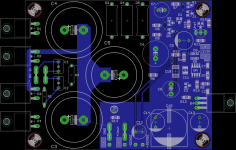
The red layer is a routing layer with the in-between empty areas "filled" with ground metallization. The blue layer is more or less a plane of ground metallization. But I'm with you: I too would like to see a few jumper wires across those two southwest-to-northeast diagonal tracks on the blue layer.
On the red layer, yes. On the blue layer it's a pretty good approximation of a plane. The reason why it renders in the color "pink," is that both red and blue are present.It is not a ground plane, it is a random bunch of bits of copper connected together.
The red layer is a routing layer with the in-between empty areas "filled" with ground metallization. The blue layer is more or less a plane of ground metallization. But I'm with you: I too would like to see a few jumper wires across those two southwest-to-northeast diagonal tracks on the blue layer.
Last edited:
Hm, ok. The red copper pour is useless then.
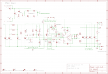
Also I see you use remote sense. If you want to use this to compensate the impedance of both wires to the load, you'll need to reference the negative terminal of the voltage reference to SENSE- (or use a true differential amplifier).
Anyway, the negative terminal of the reference, and the ground connection of the feedback network (ie, R13) ALWAYS need to be connected to the same point, without any extra current going there.
This is because the opamp will apply its gain (Rx/R13 + 1) to what it thinks is Vref... and that includes any voltage between reference negative terminal and R13.
In this schematic your VREF is referenced to local regulator GND, HOWEVER the feedback network is referenced to the load GND, so the voltage drop in the GND wire is actually going to be amplified by (Rx/R13 + 1) ... 😀
I'm not really fond of remote sense, it is tricky to get a good stable response, cable parasitics can be a problem, and the sense wires make nice antennas...
Also C13 combined with the sense cable impedance, introduces an extra pole in your openloop response, this can be nasty.
WHat kind of caps are on the board to be powered ?
It is not possible to design a regulator without knowing what capacitors are going to be on its output. That includes the C, ESR, ESL and the inductance of the connection between everything. All this is part of the same circuit and should be designed together.
The less you know, the more compromises you gonna have to make (mostly in adding resistance somewhere, real or synthetized with feedback). If you need unconditional stability, you gonna have to make some compromises you're not gonna like. And it's not gonna be really unconditional either...
WHat kind of caps are on the board to be powered ?
Hi Peufeu, thanks for taking an interest in my little project which continues to be an enormous learning exercise for me under Mark's tutelage.
The load will be a computer motherboard. Between the PSU rails and this load is my 'ATX power control board' for wont of a better name. The ATX power supply guide provides guidance as to the amount of load capacitance the PSU must handle, but of course it will vary from board to board. In any event, the resistance and inductance of 6 inches of wire was enough to provide a healthy buffer and cure the issues I was getting in my modelling when I merely added a lump of load capacitance.
It is not a ground plane, it is a random bunch of bits of copper connected together.
This obscures the layout and prevents you from seeing the path the current will actually take between two "GND" pins. Since this copper pour is cut everywhere in tiny pieces by other signal traces, the "GND" path may be very convoluted and lead to common impedance coupling, but it is very difficult to see.
If you want a decent ground plane, you can do a proper copper pour on layer 2, with no traces in it.
As Mark noted, I poured both the top and bottom layers.
Hm, ok. The red copper pour is useless then.
Don't forget there are ground connections from SMD parts J1, Z1, Vref (depending on which part is populated), C10, C11 as well as the through hole components (C8, C12, Vref, the output caps and the LED). I presume the alternative is to place vias to drop their ground connections straight down to the bottom layer?
Is there a cost attached to pouring the top? It's monetarily free to implement.
Attached is a pic with the top layer of the board turned off to better highlight the copper pour on the bottom layer. (I haven't yet implemented Mark's suggestions.) The traces on the bottom layer are relatively minimal (let's come to the Sense routing below).
The largest hole is the clearance around a via. But you don't need that for your power supply. Just visualize the currents through "GND" and do the layout so they don't end up on the sensitive spot, which is the point where the reference ground, feedback network, and output ground join together.
I have to admit that you've lost this newbie here but I will give it some more thought
But I'm with you: I too would like to see a few jumper wires across those two southwest-to-northeast diagonal tracks on the blue layer.
Ok so I take it the concern is the area around R6 where the ground plane/pour is partially dissected. The interruption closer to C12 can be improved by shifting C12 higher.
At one point I was going to move the sense connections and input cap up closer to D3/D4 but left them where they are because it is easier to jumper them to the Vout connections to disable sense.
Also I see you use remote sense. If you want to use this to compensate the impedance of both wires to the load, you'll need to reference the negative terminal of the voltage reference to SENSE- (or use a true differential amplifier).
I blatantly copied the typology of the Jung/Didden regualtor here. Their LM329 is referenced to the regulator board ground and not SENSE-. (I hope I am understanding your comment correctly.
Anyway, the negative terminal of the reference, and the ground connection of the feedback network (ie, R13) ALWAYS need to be connected to the same point, without any extra current going there.
This is because the opamp will apply its gain (Rx/R13 + 1) to what it thinks is Vref... and that includes any voltage between reference negative terminal and R13.
In this schematic your VREF is referenced to local regulator GND, HOWEVER the feedback network is referenced to the load GND, so the voltage drop in the GND wire is actually going to be amplified by (Rx/R13 + 1) ... 😀
I'm not really fond of remote sense, it is tricky to get a good stable response, cable parasitics can be a problem, and the sense wires make nice antennas...
Also C13 combined with the sense cable impedance, introduces an extra pole in your openloop response, this can be nasty.
Re the last point, do you mean C12?
I have to admit I decided to add the sense capability because I perceived it to be an easy add on (following the Jung/Didden reg as mentioned above). In all my stability and other modelling I have not included C12 and the sense setup. That is, the feedback network samples Vout. A big mistake?
In my implementation I really can't sample the load in a proper sense fashion. I can merely take the sense from the control board (see link above). If the pass transistors on the control board are shut off there is no voltage beyond that point and they only turn on if the voltage rails are up to voltage spec. Perhaps this makes its implementation completely pointless but I was thinking it costlless to implement the changes to the two boards (bar the cost of one cap and a few connection pins) and easy to run 3 strips of coaxial cable.
Abandon and simplify?
Thanks!
Steve
Attachments
Last edited:

Thanks. I guess the question regarding the sense of Sense looms large over this.
I can avoid the need for the lower 3 jumpers by shifting C12 towards C5, routing the Vout trace below the Sense input pins and shifting the latter up a bit to make room for this. With one extra via, the long bottom layer trace from Q1 to C9 can be shortened a lot thereby potentially avoiding the lowermost of your three airwires in the middle.
Question: I have avoided placing vias underneath electrolytic caps due to their metallic exterior; is this caution sensible or unwarranted? (The vias won't be tented if I pay for the basic service from the likes of SeeedStudio.) Under the can will reduce the bottom layer portion of the trace from Q1 to C9.
Also, the tee from the right side of the ground pin of C5 down to the plane; I can easily make this spur on the top and bottom layers if that helps.
> I blatantly copied the typology of the Jung/Didden regualtor here.
> Their LM329 is referenced to the regulator board ground and not SENSE-.
Hm, check the schematic, it is referenced to SENSE-...
http://www.linearaudio.nl/linearaudio.nl/images/pdf/superreg_article.pdf
> Re the last point, do you mean C12?
Yes C12 adds a pole in the feedback.
> I have to admit I decided to add the sense capability because
> I perceived it to be an easy add on (following the Jung/Didden reg as mentioned
> above). In all my stability and other modelling I have not included C12 and
> the sense setup. That is, the feedback network samples Vout. A big mistake?
Remote sense is tricky. You could model it by adding wire parasitics. But the main problem is sense wires picking up EMI (if this goes inside a PC, that could happen).
The trick is to not make the regulator too fast. The wire inductance on the output reduces the capability of the output transistor to respond quickly to current variations. This introduces an extra pole, or at least lowers the output transistor pole frequency and reduces phase margin. If the opamp wants to react too fast, it will fight the wire inductance and this will result in peaking and/or reduced staility, so the compensation components should be considered carefully. You could add a small capacitor between the regulator output and the feedback divider midpoint, but it may not be needed and its value is not easy to determine in simulation (unless you know all wiring parasitics).
Personally for powering a PC, I would use a switcher like a PicoPSU.
Next solution would be a switcher which outputs a voltage about 0.2V too high, and a linear LDO post-regulator.
Another solution would be a linear PSU which outputs a voltage about 0.2V too high (with big heatsink but no need to optimize the regulation), and a linear LDO post-regulator.
The idea being that the LDO post-regulator drops 0.2V, so with 5A it will dissipate 1W, that can be done with an opamp and a SMD MOSFET, or a thru-hole one with a very very small heatsink, and you can stick that on your ATX power connector, which means it can do 4-wire force/sense on the mobo without wires. The LDO MOSFETs also act as load switches.
That's what I'd do... just throwing ideas, not sayin you should scrap your design, ok ?
> I blatantly copied the typology of the Jung/Didden regualtor here.
> Their LM329 is referenced to the regulator board ground and not SENSE-.
Hm, check the schematic, it is referenced to SENSE-...
http://www.linearaudio.nl/linearaudio.nl/images/pdf/superreg_article.pdf
Hmm. Have a look at the schematic here. In any event, I botched slightly the implementation versus this anyway. In terms of "equilalent components":
My R10 = Jung/Didden (my link above) R5 whose input is taken from reg Vout. This point was discussed in Jung/Didden reg thread at one stage. Because I have a Mosfet I have input from Vin for the 12V rail while 12Vout feeds Vref and the op amp supply for the 5V and 3V3 rails.
My Vref = D5 (note, referenced to reg GND)
My R11 and C8 = R4 C9 (note, referenced to reg GND)
My C12 is where I went wrong versus this schematic, plus Jung/Didden R16 and C12: I did not implement but could easily
Jung/Didden C3 was not needed to stabilise the circuit (I am using Ry and Cy to stabilise)
Yes C12 adds a pole in the feedback.
As above
Remote sense is tricky. You could model it by adding wire parasitics. But the main problem is sense wires picking up EMI (if this goes inside a PC, that could happen).
Even with screened wire?
The trick is to not make the regulator too fast. The wire inductance on the output reduces the capability of the output transistor to respond quickly to current variations. This introduces an extra pole, or at least lowers the output transistor pole frequency and reduces phase margin. If the opamp wants to react too fast, it will fight the wire inductance and this will result in peaking and/or reduced staility, so the compensation components should be considered carefully. You could add a small capacitor between the regulator output and the feedback divider midpoint, but it may not be needed and its value is not easy to determine in simulation (unless you know all wiring parasitics).
Hmm. Starting to sound like I should drop it although presumably the Jung/Didden regulator faces the same issues without knowing all permutations as to how it will be deployed. If it still makes sense to use it I need to check my models as I effectively don't have C12/R16 filter on Sense+.
Personally for powering a PC, I would use a switcher like a PicoPSU.
Next solution would be a switcher which outputs a voltage about 0.2V too high, and a linear LDO post-regulator.
Another solution would be a linear PSU which outputs a voltage about 0.2V too high (with big heatsink but no need to optimize the regulation), and a linear LDO post-regulator.
The idea being that the LDO post-regulator drops 0.2V, so with 5A it will dissipate 1W, that can be done with an opamp and a SMD MOSFET, or a thru-hole one with a very very small heatsink, and you can stick that on your ATX power connector, which means it can do 4-wire force/sense on the mobo without wires. The LDO MOSFETs also act as load switches.
That's what I'd do... just throwing ideas, not sayin you should scrap your design, ok ?
Understood and ok. 🙂 At the moment I have a mini PicoPSU (i.e. the one that plugs directly into the ATX power socket on the motherboard) fed 12V from a capacitor input filtered 12V Mosfet-based regulator from Fidelity Audio. Various people have found improvements replacing the PicoPSU with a multirail linear PSU.
This project started there as a platform for learning something about electronics. I've learnt a lot. I'm hoping I am making progress...
Last edited:
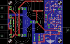
The attached image highlights peufeu's point re how useless the top layer copper pour is. For the SMD parts it would seem more appropriate to route their GND connections to the bottom layer with either top layer routing to nearby through-hole component GND pins or vias.
Attachments
Ok I've decided to drop the Sense implementation and move on. Peufeu's comments regarding the ground reference for Vref seem to make a lot of sense. While this issue, plus the pole created by the filter for +Sense input, surely also affect the Jung/Didden regulator (as per the latest schematic unless that is simply incorrect) when coupled with the fact that my sense point isn't right at the load and the fact that I have already bitten off a far greater level of complexity than I initially intended I think it's wise to drop it and move forward. I've still got a lot to do even once this thing gets off paper. Removing the Sense functionality will simplifiy the ground plane issues as well.
You guys are probably still laughing at my goals with this project. Yet even with no improvement as a result of the power supply I feel the task has already been and will continue to be very educational. I continue to read Cordell and Self (as well as the Art of Electronics) and look forward to future projects.
Thanks for all the help so far!
- Status
- Not open for further replies.
- Home
- Amplifiers
- Power Supplies
- Adventures with 5A regulated voltage circuits