I'm using my LT30xx based "SilentSwitchers" (https://www.diyaudio.com/community/threads/silentswitcher-mains-free-15v-and-6-5-3-3v-power.297147/post-6944374). So I have +-15V, +-12V and +-9V versions. All have very low noise (about 1uVrms from 10Hz-100kHz).
IME Silent switchers can pass along common mode ground noise from wall warts, mostly up around 1-2Mhz (at least for my wall wart).
Somehow I don't think you know what a Silent Switcher is; otherwise you would know that a Silent Switcher and a wall wart are not necessary related.
Gosh, you fellows are tough on a guy. Gave you the short story on Silent Switcher before. There is a bit more I left out the first time: Jan Didden used to sometimes promote SS as convenient to use with a wall wart. He described it as a good low noise solution without any caveats. So, I acquired two of the devices and tried one as suggested. Found a noise problem in the SS powered load device. Problem was traced to WW noise as previously described. Other WW exhibited same problem as the first one.
Then tried SS with USB battery pack since maybe that would be okay. Found that battery pack had an internal SMPS 5v regulator with noise appearing on the USB output. Traced RF EMI from battery pack along USB cable to SS, then continuing along to load circuit. Not as bad as WW since battery pack had no ground return path, but still not as clean as I had hoped.
Cleanest power resulted from powering SS from clean 5v linear supply.
Sorry for the long winded story. Now see that a terse comment about a possible noise source could be taken for something other than was intended.
Basically, the USB cable from linear 5v power supply to SS was swept for radiated RFI/EMI. No discernable EM radiation was found above normal ambient room levels. For audio work the linear supplies are powered from a used Monster HTPS 7000 Mkii power conditioner (which was designed by our own 1audio and Richard Marsh). That helps clean up AC line RFI/EMI quite a bit.
You also have to remember that my LT30xx switcher is not the same as Jan's SilentSwitcher. The functionality is the same but the designs are not related. It is like calling all linear supplies same as yours.
This week I did some testing on my ES9822PRO adc. With its lower noise floor I was able to do some THD+N optimization on my AK4490 and ES9038Q2M dacs. After some iterations I found the optimal solution for both dacs: the lowest THD+N requires to feed VREF directly from LT3042. So forget about AVCC/VREF op amp buffers (ES9038Q2M) or large VREF capacitors (AK4490).
My earlier result with ES9038Q2M can be seen here. THD+N (-110dB) was quite far from datasheet (-120dB).
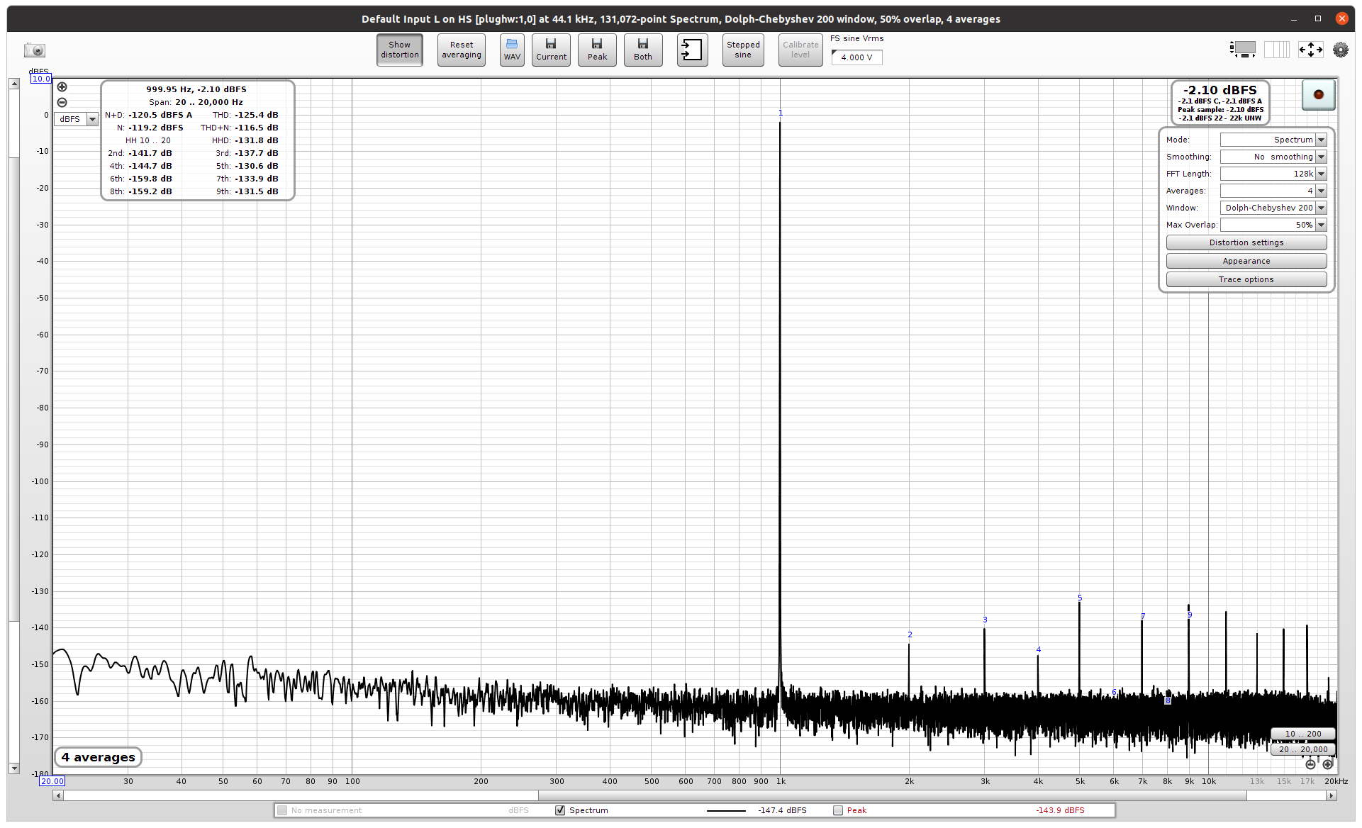
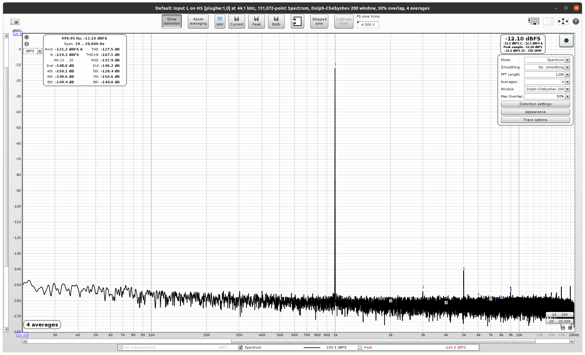
Today I took out the op amp buffer and connected LT3042 directly to AVCC, AVCC-L and I/V VREF. Here are the results with THD C2+C3 compensations:
0 dBFS input

So THD+N improved to -116.5 dBFS. With a more proper layout I would expect to squeeze 1 or 2 dB more out of this. The higher harmonics are unfortunate but typical of ESS chips.
-10 dBFS input

The 5th harmonic may be due to ADC as I see the same with AK4490. I have not yet done any THD compensations of the ADC.
To summarize: for optimum performance discard all suggestions made by audiophiles.
My earlier result with ES9038Q2M can be seen here. THD+N (-110dB) was quite far from datasheet (-120dB).
Today I took out the op amp buffer and connected LT3042 directly to AVCC, AVCC-L and I/V VREF. Here are the results with THD C2+C3 compensations:
0 dBFS input
So THD+N improved to -116.5 dBFS. With a more proper layout I would expect to squeeze 1 or 2 dB more out of this. The higher harmonics are unfortunate but typical of ESS chips.
-10 dBFS input
The 5th harmonic may be due to ADC as I see the same with AK4490. I have not yet done any THD compensations of the ADC.
To summarize: for optimum performance discard all suggestions made by audiophiles.
haha, you are darn right, a high-performance needs the understanding of physics but not just a faith in the red wima magic or so ))To summarize: for optimum performance discard all suggestions made by audiophiles.
9038Q2M requires a very low-ESR wide-band Ref regulator and you have nearly zero chance to find some suitable LDO for that. The best way using an opamp as "super-regulator" as in 9038Q2M appnote. One more point, 9038Q2M and 9822 contain the precise oscillator onboard, nearly any $1/10 Epcos-crystal +2 caps and res 0402 will provide an unbeatable low jitter clock. All these things I told years ago in the "ES9038Q2M boards" but nobody cares.
Seems to me that LT3042 fits the bill. Which 9038Q2M appnote are you referring to?9038Q2M requires a very low-ESR wide-band Ref regulator and you have nearly zero chance to find some suitable LDO for that. The best way using an opamp as "super-regulator" as in 9038Q2M appnote.
I do not like those high order harmonics in post #1489. I want to avoid them in my amplifiers and I am not interested in an ADC/DAC system that adds them artificially. This is not good. Background must be free of high order harmonics down to -140dBr at least, otherwise the system is useless to me.
Maybe it was my poor implementation but that "super-regulator" was what I had on the board before. Taking it out improved THD+N by 5 dB.ES9038Q2M SKT VER 1.0.2.pdf
Many DACs/ADCs have increased high order harmonics near full scale. As you can see from the other graph they are much lower with lower signal level.I do not like those high order harmonics in post #1489. I want to avoid them in my amplifiers and I am not interested in an ADC/DAC system that adds them artificially. This is not good. Background must be free of high order harmonics down to -140dBr at least, otherwise the system is useless to me.
My (now removed) ref was also OPA1612. Like I said my implementation was probably poor. Another thing is that there is quite a lot of variation between ES9038Q2M chips.I got THD+N -124db with dual 9038Q2M, and the ref was opa1612.
@bohrok2610,
Thank you for these measurements.
It seems to confirm what I had speculated about (for ESS DACs) that this typical error patterns we see are result of glitch energy wandering around when the converter excercises more than one of the 64 current cell segments (the thermometer-coded 6 bit final output current sources).
1/4th the final converter speed ==> 1/4th of glitch energy per time unit ==> 12dB lower levels in spectrum, theoretically. And higher noise. In DSD mode I saw the noise also goes up and the hash seems to go down as well.
Someone has said here(?) that an ESS I/V stage is best realized with a passive filter in its first stage to fully isolate the OpAmp wrt RF glitch energy. I would fully agree (and I'm working on that front, too, also adding shunt caps -- to rails and between +ive and -ive chip output pins). Remaining errors from the glitching should be then down to the base level the chip is really capable of. Which might even be improved by playing with the output pin node voltage (as set by the I/V) and other fine tuning, besides HD2/3 compensation, stiff Vref etc.
In extreme cases the glitch energy corrupts the output to the point that the "ESS hump" is really sticking out in the typical THD+N or IMD vs level plots.
See my investigation here: https://www.audiosciencereview.com/...-hump-revisited-khadas-tone-board-v1-3.30136/
However, for the ESS ADCs not that many options, except lowering the clock. Lowering levels helps for both DAC and ADC but is awkward, of course, with < FS/64 as the target.
- Home
- Design & Build
- Equipment & Tools
- ADCs and DACs for audio instrumentation applications