Software experience (and ways of thinking) generally maps very poorly to HDLs, basically because most programming languages have a built in notion of sequence and hardware description languages only look like they do.
Verilog also looks FAR too much like C, which is a massive trap because it is nothing at all like C.
Verilog also looks FAR too much like C, which is a massive trap because it is nothing at all like C.
Software experience (and ways of thinking) generally maps very poorly to HDLs, basically because most programming languages have a built in notion of sequence and hardware description languages only look like they do.
Verilog also looks FAR too much like C, which is a massive trap because it is nothing at all like C.
Verilog is a trap, yes. I do still like it better than VHDL syntactically. I'm rubbish at both but being someone who learned C first, I still prefer the Verilog syntax.
So, since I don't see any software based (with minimal hardware) SPI to I2S conversion available, it appears the CPLD solution is the only path... so I started a few weeks ago studying Verilog. One of the most frustrating experiences I ever had... my 30 years of pro software experience is worth shite, or even worse, it's actually a hurdle to work around. Nothing seems to be familiar, other than the Verilog language syntax... I can read some basic code and figure out how it's working, but when it comes to implementing anything, I am still very far away and in the dark, struggling with the very basics of behavioral description...
The Internet is full of examples, comments, advice, boards, etc... but somehow nothing is coming together as a coherent way to approach a dgital design from scratch, starting from defining the inputs and the outputs. It's funny, If I would have to design a Moore state machine with pen and pencil, as I was educated, with a bunch of flip flops and gates, I could probably do it much faster than thinking through it's behavioral description, I suppose my brain is not wired for this (or is too old to process and digest the required information).
But I'm not ready to give up yet...
I've never tried it, but I think Vivado and Quartus Prime can do HLS, where you can write what you want in C or C++ and it'll synthesize it for you. I have no idea how well it works and what level of license it requires.
basically because most programming languages have a built in notion of sequence and hardware description languages only look like they do.
That much I got early in the learning process, HDL code is edited and looks sequential, but is executed in parallel.
What I'm missing is an integrated approach to the design process, from the problem definition, to splitting into modules, to the final implementation. Otherwise, I went through lots of tutorials, they all address only a local little problem, like "edge detection", "delay by one clock", etc... How do I put these together to get a functional result, itcrossing is still a mystery to me. The clock domain scare, that no simulation will help with, always hangs over the designer's head, not even a synchronous clock divider is 100% safe, without extra counter measures (like syncing the output).
For example of a stupid problem I can't figure out, I have a [63:0] register and two [31:0] registers, how do I copy the 32bit registers to the 64bit register, on the posedge of a clock, so that after 64 clocks I have the copy operation complete? After 2 days of banging my head, nothing that I tried doesn't even compile...
Sounds to me like you have a 64 bit register and two single bit signals? Not two 32 bit registers?
For the register case why on earth would this take 64 clocks, that's just nuts. I think that case is a single clock operation.
The integrated design process here is just the same as what you would use for any digital logic, there is nothing special about describing it in HDL except that that is less painful at scale then drawing schematics.
One design hint, one clock and clock enables usually trumps clock dividers unless clock dividers are part of dedicated hardware, generate the clock enables from a more machine and have all the actual logic look like (VHDL)
if rising edge (clk) and clk_en ...
This takes advantage of the fact that a CLB usually has a clock enable input right to the flipflops, and this way everything stays syncronous. Don't make clk and clk_div_64, run the whole mess off your clk and just have a divider that produces a clock enable pulse every 64 clocks. Your clock routing is a limited resource, and this way your timing tools will actually work.
Sounds to me like you have a 64 bit register and two single bit signals? Not two 32 bit registers?
For the register case why on earth would this take 64 clocks, that's just nuts. I think that case is a single clock operation.
See what I mean? That's not how's supposed to work. The 64 bit register needs to be filled with the 2 x 32 bit registers in a synchronous mode. The closest I can think of is a 64 bit shift register that clocks out the first 32bit then the other 32 bits. That is, it takes so deep into the implementation to define the behavior that I'd rather draw the schematic 🙂.
And yes, I was hoping the behavioral description to save some schematic drawing, but I may take the other route, draw a schematic with standard IEEE components, and use the tool as a simulation/verification and implementation. Verilog coding the behavior without visualizing the schematic would be the whole shtick, otherwise what's the point of making an extra abstraction effort?
Do I need to add, "I hate it"?
I have no idea how well it works and what level of license it requires.
No clue myself, but then the Vivado HLS Lite is free. Certain limitations, it's tied to certain boards, but it's a great tool for learning. But then HLS would be the last drop that would transform this learning process into a total chaos.
You are describing implementation details, hence why you are winding up down at shift register level.
I also suspect that 'register' may possibly not mean quite what you think it does in this context.
What are you actually trying to achieve here?
I also suspect that 'register' may possibly not mean quite what you think it does in this context.
What are you actually trying to achieve here?
You are describing implementation details, hence why you are winding up down at shift register level.
I also suspect that 'register' may possibly not mean quite what you think it does in this context.
What are you actually trying to achieve here?
Once again, that’s my big problem, how to describe the functionality before writing the code (or drawing a schematic). Story board?
The inputs are two entities (call them L and R) able to clock out 32 bits of data. I want a single output, always clocking out 64 bit of data, first the 32bit L then the 32 bit R. The extra requirement is that clock goes first to L (R is idle, not clocked) then to R (and L is idle, not clocked). I can have as an input a clock/64 signal, but then I’m afraid of using it to signal switching from L to R clocking, since it looks to me like clock domain crossing. So I’d rather count 32 clocks and then switch over to clocking the other (L/R) input with the following 32 clocks, etc... if that makes sense.
So your inputs are single wires L,R.
Your outputs are O,Clk_L, Clk_R, LR_Clk or something of that sort?
Clock input is 64Fs?
At heart this is just a mux, no need for registers at all (Apart from in a 6 bit counter), well maybe a single flipflop to deglitch things and make everything synchronous but you probably don't really need it.
I think you need all of 6 flipflops for a 6 bit counter to do the divide by 64, with the top bit of that counter deciding which input you route to the output and gating the clock to the appropriate pin, top bit of the counter also forms your LR output.
The clock gating to the output will be a little device specific, if you have DDR output drivers that is often a nice way to skin it, but that usually means FPGA rather then CPLD.
Note that everything is synchronous to that 64Fs clock, and if you pick the correct edge (check the ADC datasheet) you should have plenty of setup and hold time.
Really, your block description is inputs, outputs, clocks, and a timing diagram.
Last edited:
So your inputs are single wires L,R.
Your outputs are O,Clk_L, Clk_R, LR_Clk or something of that sort?
Clock input is 64Fs?
At heart this is just a mux, no need for registers at all (Apart from in a 6 bit counter), well maybe a single flipflop to deglitch things and make everything synchronous but you probably don't really need it.
I think you need all of 6 flipflops for a 6 bit counter to do the divide by 64, with the top bit of that counter deciding which input you route to the output and gating the clock to the appropriate pin, top bit of the counter also forms your LR output.
The clock gating to the output will be a little device specific, if you have DDR output drivers that is often a nice way to skin it, but that usually means FPGA rather then CPLD.
Note that everything is synchronous to that 64Fs clock, and if you pick the correct edge (check the ADC datasheet) you should have plenty of setup and hold time.
Really, your block description is inputs, outputs, clocks, and a timing diagram.
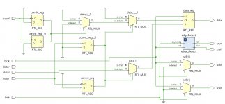
Thanks, using muxes was a good clue, they map to if/else Verilog clauses. I got a small breakthrough, the SPI (slave) to I2S (master) converter is completed, schematics are attached. The converter receives BCLK and LRCK from the XMOS chip. It generates on the pos and neg edges of the LRCK single pulses (CNVL, CNVR) to start the conversion, which completes (for the LTC2378, which has an internal asynchronous clock) in 675nS, well before the LRCK flips again. So for each half of the LRCK, one ADC gets the start pulse and completes the conversion, the other one is clocking out data (e.g. DATAR) to DATA, the output to XMOS. Then the roles are swapped, the second ADC does a conversion and the first clocks out data (DATAL), etc... Just for the safety, there's inputs for the conversion complete signals (DRDYL, DRDYR) from the ADCs which are used to validate the data.
The only thing left to do is delay the DATAL and DATAR by one clock period before clocking out to DATA, to comply with the I2S standard. As it is right now, the output is Left Justified. Not a big deal (I would think?).
Then writing a solid test bench to test this thing. That will be yet another learning curve...
Last edited:
It does what you describe, but not quite I think what you want!
Specifically, normal stereo usage has both channels sample simultaneously, not offset by half a sample period.
Regards, Dan.
Specifically, normal stereo usage has both channels sample simultaneously, not offset by half a sample period.
Regards, Dan.
It does what you describe, but not quite I think what you want!
Specifically, normal stereo usage has both channels sample simultaneously, not offset by half a sample period.
Regards, Dan.
True, but this is for instrumentation, not for music. With sampling simultaneously two channels on SAR ADCs I think it's very difficult (if possible at all) to create an I2S stream, since there's no time slot for acquisition (when the output needs to be idle). Clocking out data (previous sample) during a new acquisition is very bad for performance (all data sheets for competitive SAR ADCs able to work this way (some don't) are mentioning this).
Separate sample times for the two channels will make phase measurements really challenging. Is there a way to buffer the SPI to handle the data formatting? Can you have both sample at the same time and read back both data in the available window allowing for internal settling etc?
Another obscure option is to see if the XMOS supports dual wire AES in (an older way to move high sample rate audio). Then you could handle each ADC as independent. Another possible interface would be TDM.
Another obscure option is to see if the XMOS supports dual wire AES in (an older way to move high sample rate audio). Then you could handle each ADC as independent. Another possible interface would be TDM.
Can't you just buffer one or two samples ahead of time? That way you can acquire the data from the ADCs in the preferred method, buffer a sample then output it as per I2S? Or am I misunderstanding?
Guys, there is a fundamental delta between I2S and SPI. While I2S is a streaming protocol, SPI is a bursting protocol. To add insult to injury, a delta-sigma ADC natively streams out bits, while a SAR ADC is not, since it’s principle is a binary search through all quantization levels, before defining the digital output. Therefore, whatever way you dice it and slice it, at a moment in time you will find out there’s nothing new you can clock out during the required conversion time, while you cannot pause the I2S streaming. Not to mention that clocking out during conversion is a big nono, for SNR performance reasons, in all ADCs that supports it.
A FIFO (dual port RAM) is probably a solution, since the data rates would be still the same on both sides (XMOS and ADCs), but that would blow the complexity out of a small CPLD right into the FPGA world, where a FIFO IP would cost real money, or requires an extra dual port RAM, which is anything but cheap too. See for example https://www.cypress.com/file/38166/download Even more, FPGAs are nothing like an XMOS chip, you can’t just buy the FPGA chip, solder it on your board, and do a on board programming, all that for free. Such a process requires a rather big investment, in software and hardware, that I’m not ready to get into. And guess what, a FIFO could introduce an additional latency, something that really could be of interest to measure, on each channel.
Otherwise, I don’t ever remembering having any reason for doing any phase comparison between channels, either in the analog or digital domain, in fact my Rohde UPD doesn’t even have such a feature. Also I haven’t seen such a feature in any PC based audio analyzer software (could exist, though) and I really wonder what would such an inter channel phase measurement tell? It could not allow using an hypothetical instrument with shifted sampling to precisely position a microphone right into the sweet spot of a stereo setup, but I could live without such a feature.
Good point though, I’ll check if my UPD has any phase shift between channels.
Last edited:
My acoustic software cares a lot about phase shift between channels since it emulates a 2 port VNA in effect. My Shibasoku also can measure interchannel phase as can the AP stuff. its less of an issue with most modern digital stuff but I have encountered wireless audio links with serious interchannel phase instability.
Other PC audio that does measure or use phase would be ARTA, REW and Virtins I seem to remember. They may not present it but need it to show delay accurately.
Other PC audio that does measure or use phase would be ARTA, REW and Virtins I seem to remember. They may not present it but need it to show delay accurately.
Buffer ahead of time is what every I2S ADC actually does, it goes something like this....
You have two 32 bit shift registers and one 64 bit shift reg.
Your cycle is 64 clocks as usual.
On the first edge you start both ADCs converting, you also transfer the contents of the two 32 bit shift registers to the 64 bit one in the appropriate order over a parallel link.
You then stop the SPI clock for 32 cycles.
Next you clock the SPI buses 32 times transferring the ADC samples into the two 32 bit shifters.
Meanwhile your 64 bit shifter is shifting out the 64 bits of samples.
A common trap that people regularly fall into is upside down LRCLK which causes an LR channel swap but also a one sample offset.
- Home
- Design & Build
- Equipment & Tools
- ADCs and DACs for audio instrumentation applications