Well, I guess he wanted to explore the THD limits of his circuit. The thread in this forum contains only a part of his experiments from the Ukrainian forum.
As regards the Yewen version, with a THD of -152dBc @ 3Vrms while driving a 30 Ohm load, I see it as a very good candidate for an output driver to the Victor's oscillator, at least in my humble THD measurement setup.
As regards the Yewen version, with a THD of -152dBc @ 3Vrms while driving a 30 Ohm load, I see it as a very good candidate for an output driver to the Victor's oscillator, at least in my humble THD measurement setup.
This in the funniest thing I've ever seen with Mouser. They shipped 10pcs of CS43198 in DFN (they provided the UPS tracking number) while the quantity is still reported as 17 available. I hope they did not ship the wrong parts. I'll find out tomorrow.
Got the strip of 10 CS43198 chips today, they are perfectly fine. Mouser site still shows 17 chips available https://www.mouser.ca/ProductDetail...=sGAEpiMZZMv0NwlthflBi1xF5vPbfHdc7dHmfccCwII=, looks like the miracle of the five loaves and two fish, XXI century version. More DAC fun to follow!
About composite amplifiers, here's a very simple old technique that I experimented with. It can be easily designed, analytically or by simulation, for any closed loop gain. The only precondition is to have an accurate AC model for the op amp(s), which is usually available today (the models distributed for free suck at transient (large signal) analysis, being otherwise quite accurate).
Very interesting, thanks for sharing!The idea is pretty obvious: a composite amp, designed as a low pass filter of n-th order, with the additional constraint for the overall filter transfer function to be stable, which is if and only if all its poles are inside the unit circle in the Z plane. Known filter coefficients can be used, so the design is simple.
I did not try over n=3, but I suspect the sensitivity increases quickly with the filter order, to the point where the natural op amp AC parameters variations become critical and everything turns into a gamble.
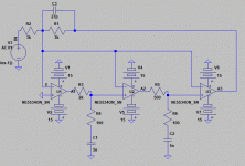
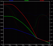
Did a quick sim of a 3-stage design with NE5532 models from S-Audio.Systems // SPICE models (see also https://www.dialog-semiconductor.co...ultra-low_power_rail-to-rail_cmos_op_amps.zip).
I've added "fun caps" to bring up the composite Aol even more at lower frequencies.
Appears to be neatly stable in a crude Aol sim as well as in a transient sim, I did not expect that due to the pole-zero phase kink in the 5532 Aol.
Attachments
This is surprisingly awesome, simple, and cheap.
I'm going to do a nested loop power amp, so I'm taking notes.
I'm going to do a nested loop power amp, so I'm taking notes.
Building an audio power amp based on Yewen's idea will provide only a marginal performance improvement (if at all) over other loop gain increase techniques. This is because of the limited output stage bandwidth and its inherent limited phase margin.
To my experience, Yewen's technique is effective for fixed gain, inverting, composite op amps only. An ultra low distortion state variable oscillator would IMO benefit most from Yewen's technique.
For DAC output, there's no need for this; a combination of OPA1611 with a high current buffer will do the job nicely; due to the very high bandwidth of the high current buffers and unity gain, no extra compensation is required.
I'm going to do a nested loop power amp, so I'm taking notes.
ZD-50. Based on this same Yewen paper
My ZD-50 ultralow distortion chipamp.
Last edited:
Building an audio power amp based on Yewen's idea will provide only a marginal performance improvement (if at all) over other loop gain increase techniques.
Certainly, it's not a technique for a power amp.
But seeing clever designs sure improves motivation 😀
> This is because of the limited output stage bandwidth and its inherent limited phase margin.
Yeah, I've been wondering for a while how to boost that bandwidth. Plenty of ideas in SPICE, I'll check them pretty soon. I dusted off the network analyzer this evening.
ZD-50. Based on this same Yewen paper
Hmmm, it looks a bit complex, I wonder how he tuned all the values in there...
Attachments
That's a typical Russian design. I'm sure it works fine in the authors hands, but I would myself never build something I don't fully understand to the last detail. To me, a simulator is like a sophisticated calculator, very useful, but never a replacement for a brain.
Anyway, I would think performance and stability would be extremely PCB layout dependent.
Anyway, I would think performance and stability would be extremely PCB layout dependent.
This one looks far more Yewen'ish than the above:
Attachments
Last edited:
To me, a simulator is like a sophisticated calculator, very useful, but never a replacement for a brain.
+1
This evening I've setup the scripting for the network analyzer and the new programmable power supply. Still waiting for that damn STM32, and I'll have frequency response and phase while stepping DC output voltage and current. I am quite curious to see how accurate those power MOSFET spice models are...
That's a typical Russian design.
Ukrainian 🙂
But he lives in USA many years.
I'm sure it works fine in the authors hands
Many peoples were very satisfied building this amplifier, mostly with the author's PCB, but some make their own.
Anyway, I would think performance and stability would be extremely PCB layout dependent.
Yes, this is correct. Author's PCB is 4 layers very well layouted design.
I decided to give an OPA1612 + 2 x BUF634A (per channel, a total of four) composite a shot for the ES9038PRO I/V. BUF634A is as cheap as the TPA6120 and doesn’t need any stability care. OTOH the TPA6120 gain is not needed, for controlling the distortions.
After some delay due to work load, some time wasted with talking and arguing to some holes in the wall in the Digital forums, and a false start with the PCB (used the wrong footprint for the OPA1612 DFN) here's the board with the composite I/V stage, OPA1612 + BUF634A and OPA1611 output. The I/V stage layout is completely re-designed and optimized for shielding and heat sinking.
Did some preliminary measurements (before cleaning the board 😀), and the output current capability of the BUF634A (250mA) is an obvious improvement, although less than I was hoping; rather than increasing a little, starting with -6dBFS, the THD, THD+N, SINAD, and IMD are flat to the UPD instrument floor from -8dBFS to 0dBFS (4Veff output). Otherwise, overall, the distortion performance is a tad (under 1dB) worse than the OPA1622, also no hump. I adjusted the output filter (the values in the OPA1622 I/V stage I posted earlier are rendering a BW of about 25KHz, good for an audio DAC, not for instrumentation) to about 250KHz, absolutely no extra noise measured in the THD+N and SINAD measurements, these OPA161x op amps are indeed low noise.
Still to decide what version to use in the final board, but not my focus moves to designing and testing the ADC input stage, auto ranging and input protection, plus the DAC output power stage, I want this to provide at least 16Veff into 600ohm, which probably calls for a discrete design fed at +/-24V. As usual, I'll keep this thread updated.
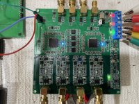
P.S. I also completed the python software for controlling the ADC board over I2C. Unfortunately the ADS127L01 does not support register control when in frame mode, but only hardware/pin mode, so I had to implement some logic and an TCA9554 I/O extender interface to I2C. Works beautiful, now I can play with the ADC without moving jumpers and flipping switches.
Did some preliminary measurements (before cleaning the board 😀), and the output current capability of the BUF634A (250mA) is an obvious improvement, although less than I was hoping; rather than increasing a little, starting with -6dBFS, the THD, THD+N, SINAD, and IMD are flat to the UPD instrument floor from -8dBFS to 0dBFS (4Veff output). Otherwise, overall, the distortion performance is a tad (under 1dB) worse than the OPA1622, also no hump. I adjusted the output filter (the values in the OPA1622 I/V stage I posted earlier are rendering a BW of about 25KHz, good for an audio DAC, not for instrumentation) to about 250KHz, absolutely no extra noise measured in the THD+N and SINAD measurements, these OPA161x op amps are indeed low noise.
Still to decide what version to use in the final board, but not my focus moves to designing and testing the ADC input stage, auto ranging and input protection, plus the DAC output power stage, I want this to provide at least 16Veff into 600ohm, which probably calls for a discrete design fed at +/-24V. As usual, I'll keep this thread updated.
P.S. I also completed the python software for controlling the ADC board over I2C. Unfortunately the ADS127L01 does not support register control when in frame mode, but only hardware/pin mode, so I had to implement some logic and an TCA9554 I/O extender interface to I2C. Works beautiful, now I can play with the ADC without moving jumpers and flipping switches.
Attachments
A sad observation: in the current semi crisis, the parts for one such board cost no less than 500 Canadian dollars (about $350). Only the two ESS chips are 300. It’s insane, it almost killed my DIY budget for this summer.
Very cool syn08, funny, opa1612AIDRGT + buf634AIDRGT composite per channel is one of the IV's i've been laying out too. but for 9028. I love these new packages. the opa1622 pinout is a dream, I hope they bring out more duals with this package and pinout. I wish the opa1612 was, the asymmetry of the old legacy SOIC8 pinout is annoying for anal retentive symmetrical designs 🙂
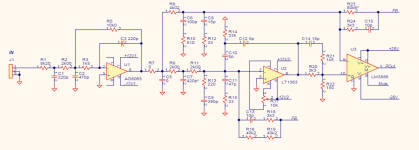
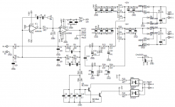
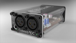
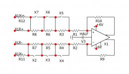
Some people asking me in PM about the ES9822 ADC project I started to develop. I moved to the simplified version for a few reason, on of them is bloody expensive $ilicon, another one overcomplicated calibration of each of 8 gain ranges + >1.5A current draw from USB. Original ADC/USB interface with UAC2 gain control(proprietary MOS-attenuator) will be released latter as Cosmos ADC Pro but so far Cosmos ADC will have DIP-switch for 8 gain-rangeses 1.7-10Vrms, without input buffers, hence, Zinput depends on the gain-range selected(from 680 to 4000ohm a fully differential XLR inputs). Due to input buffers elimination I reduced opamps rails from +/-16V to +/-6V and current consumption was reduced 7 times(also eliminated 20V rails for the MOS-attenuator!). Also, Cosmos ADC has an AUX(2.5mm jack) fully differential input 20-30Vrms to measure poweramps. In other words, the frontend is extremely simplified but the performance is extremely maximized, see attached schematic. PCM 32/44.1-384k supported. SNR/DR 124/127db(A) 2ch/1ch modes, typically, however some samples has 125/128db(A) some 123/126db(A), seems ES9822 has not too rock steady noise, actually the same as ES9038Q2M which, in fact, close to 4% I have to just throw out. THD@-.5dbfs typically 0.00003%, 3rd harmonic at -134db, 2nd -140db, others -150db and less. THD+N -120/-123db 2ch/1ch modes. I have to specify how I did measured THD+N, I made Cosmos DAC with dual ES9038Q2M THD+N -124db and DR 130db(A) but the output is filtered by LPF 1kHz 2nd order to clean up noise and harmonics >1kHz to extremely low level(I use OPA1612 as in the ADCs frontend). That way I have ultara-clean 10Vrms sine source which a lot cleaner vs my AP SYS2522. The audio-data from ADC goes to USB and next to the PC, where being send to the AP SYS2522 by SPDIF, so, the result of THD+N -123db was obtained from AP analyzer.
The clock was chosen NZ2520SD 45/49Mhz just as a cost-effective solution, this is far not the best clock, for example, Epcos SG-210STF may improve SNR of ADC up to .5db(also I did try Accusilicon oscillator but Epcos is better), however, SG-210STF has the only 24.576MHz oscillator i.e. for 48/96/192K, and 384K PCM will work in "2X mode" of ES9822 that looks a bit noisier at 100KHz and higher on the FFT. So, keeping in mind $ilicon prices, there is the NZ2520SD, which is just a little bit better than Chinese noname oscillator with ES9822, however, 12kHz "jitter test" looks anyway not too bad.
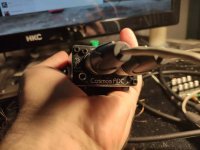
The PCB size 90x50mm, where is about 1/4 of PCB area are XLRs. The housing is extruded aluminum, fine-sandblasted, and black anodized + laser engraving. The retail is TBD but for 90% $130. Currently we try to buy the parts, and some of them have multiple 20x versus last year )) Even stupid DIP-switch got + 300% of the cost, of course, because the deficit of $ilicon 😉
The clock was chosen NZ2520SD 45/49Mhz just as a cost-effective solution, this is far not the best clock, for example, Epcos SG-210STF may improve SNR of ADC up to .5db(also I did try Accusilicon oscillator but Epcos is better), however, SG-210STF has the only 24.576MHz oscillator i.e. for 48/96/192K, and 384K PCM will work in "2X mode" of ES9822 that looks a bit noisier at 100KHz and higher on the FFT. So, keeping in mind $ilicon prices, there is the NZ2520SD, which is just a little bit better than Chinese noname oscillator with ES9822, however, 12kHz "jitter test" looks anyway not too bad.
The PCB size 90x50mm, where is about 1/4 of PCB area are XLRs. The housing is extruded aluminum, fine-sandblasted, and black anodized + laser engraving. The retail is TBD but for 90% $130. Currently we try to buy the parts, and some of them have multiple 20x versus last year )) Even stupid DIP-switch got + 300% of the cost, of course, because the deficit of $ilicon 😉
Attachments
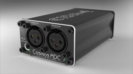
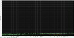
I forgot to mention the frequency response, from the left it is limited by 680ohm feedback resistors R9;10 and input caps 220uF. Right side by pole of 680ohm and 1nF + interpolation-filter of ES9822. Guys, we have to congratulate each other for the time when a cigarette pack-sized ADC just due to technology progress outperforms archaic AP/R&S etc analyzers at least in THD+N performance and cost 
Attachments
Congratulations, unfortunately the ES9822 chip and the data sheet are not available for mortals.
- Home
- Design & Build
- Equipment & Tools
- ADCs and DACs for audio instrumentation applications