Maybe finding the layout of th eTEAC VRDS20 could help you for these two chips arrangement ?
http://culture.motiontopic.net/454308334307-teac-vrds-20-cd-player-used-sold
I don't know if the longer trace for signal is a better trade off than crossing the voltage lead beneath the pcb ? Marce seems to prefer the longer path... is it important with small current leads ?
For the value of the cap, I think most of the time a trade off has to be found between the ratio and flavor in each layout.
What sort of cap do you want to use right here ? If self inductance is important and you won't put ceramic for a question of flavor (after all you could put a 4.7 X7R 603 case with your ratio, but does such an important value for a second cap would not play alone and cause more problem in relation to a slower big one ?!), you can use a two pitch throug holes size on your pcb : 2.R & 5 mm. You will be able to populate with polymer or aluminium 2 or 2.5 pitch for the bigger value and idem for the smaller (e.g. Wima MKS2 1 uf 2.5 pitch if you don't like the ceramic; note here with 1 uf the ratio is not good as this is the bigger value in 2.5 pitch with MKT).
In which forum do you share with Pedja Rodric about this circuit ?
Last edited:
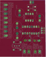
The TEAC VRDS doesn't even have a continous ground plane. It's a two layer board, And the grounds are split. Look at the photo of the VRDS-25 below. I don't know if this is an example I want to follow. This noise I'm talking about is only audible with very efficient speakers and with no attenuation. But I still find it unacceptable. I like the concept of stackable mono boards.

I was thinking of using 4,7uF and 47uF Silmic II. Of course, I could put different footprints here in order to be able to experiment with different caps.
I didn't share this with Pedja yet. It's just that the output stage is his design. Available here: Discrete Diamond Non-Feedback I/V by Pedja Rogic
I guess it would be nice letting him know before distributing boards around. 🙂
Hi, I am back home from Racal Acoustics today, so as well as getting my life back I will finally have some time to do other things than work!!!
I wouldn't get to hung up on digital and analogue grounds for a two device board, I have some ideas that I want to formulate in my head first (and I will probably copy the circuit and have a play, its much easier to do a picture than pages of text).
Anyway just to keep you on your toes, some relevant info, that I thought appropriate, instead of trying to formulate a short answer...🙂
Cos there isn't one...
http://www.x2y.com/filters/TechDay0...log_Designs_Demand_GoodPCBLayouts _JohnWu.pdf
A good article on decoupling myths and facts...
http://www.pcbcarolina.com/images/01_pcb_power_decoupling_myths_debunked.pdf
Crosstalk.
Guard traces - use 'em, or not? | EDN
Guard Traces
http://www.ultracad.com/mentor/crosstalk_coupling.pdf
http://www.ti.com/lit/an/slyt190/slyt190.pdf
http://www.ti.com/lit/ml/sloa089/sloa089.pdf
Jitter...
http://www.ti.com/lit/an/slyt179/slyt179.pdf
http://home.educities.edu.tw/oldfriend/article/SI/Crosstalk_Induced_Jitter.pdf
Ground...
http://sites.ieee.org/ctx-emcs/files/2010/09/Archambeault-Ground-Myth.pdf
Staying Well Grounded
Thanks painkiller,
I remenber this pdf now. Be aware than Mr Rodric notice : could be harder than an integrated chip ! After this design he went to OP861 for AYA2 and TDA1541 (you could find the scheme in a recent thread here or in the Audial site (pdf from 2013). People say this chip is better in standalone use than the AD844... Take a look too of the AD844 stacked thread here by George Hifi (many inputs about others chip than the PCM1704 : AD1865, TDA1541...). I saw also a thread elswhere about a video fast aop from philips in I/V conversion but don't remenber the ref !
About the Silmic 2: just tests can let you know : so you can sold sockets for jumping from a cap to an other one without solderind as it is a test board !
For me this cap is better for analogic coupling (in serie arrangement +--+)if no space for transformer or MKP...IF dc coupling is needed or pre has no serie input cap !
You try as well polymer : SAP serie from UCC, or SEP/SEPC/SEPF from panasonic... some exist in low value with better ESR than MKT and 2.5 or 2 mm pitch for a lower inductance ! I surmise the better is the layout the lower you will hear the pleasant distorsions than caps add in the set up & trade off phase of the listening test.
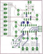
WOW the TEAC had no continous ground ! that was the 90s' years if i remmenber ! what are the aluminium caps, they looks like Black Gate standard (equal cold sound if too much used) ! near red ceramics... crystal is far from the four dac chips... and it was 2 000 euros ! 😱
Marce, didactic inputs as usual 🙂, cool...some reading for this afternoon !
Marce have you been finishing your own Subbu layout soon ? It coul be interresant to compare a full smd decoupling with one version with a mixing smd + polymer/MKT/classic alum caps... one for scope proof measurement and the other just for ears to compare where the pleasant distorsions or limiting factors are more pleasant with ears ... (sorry here OT)
I remenber this pdf now. Be aware than Mr Rodric notice : could be harder than an integrated chip ! After this design he went to OP861 for AYA2 and TDA1541 (you could find the scheme in a recent thread here or in the Audial site (pdf from 2013). People say this chip is better in standalone use than the AD844... Take a look too of the AD844 stacked thread here by George Hifi (many inputs about others chip than the PCM1704 : AD1865, TDA1541...). I saw also a thread elswhere about a video fast aop from philips in I/V conversion but don't remenber the ref !
About the Silmic 2: just tests can let you know : so you can sold sockets for jumping from a cap to an other one without solderind as it is a test board !
For me this cap is better for analogic coupling (in serie arrangement +--+)if no space for transformer or MKP...IF dc coupling is needed or pre has no serie input cap !
You try as well polymer : SAP serie from UCC, or SEP/SEPC/SEPF from panasonic... some exist in low value with better ESR than MKT and 2.5 or 2 mm pitch for a lower inductance ! I surmise the better is the layout the lower you will hear the pleasant distorsions than caps add in the set up & trade off phase of the listening test.
WOW the TEAC had no continous ground ! that was the 90s' years if i remmenber ! what are the aluminium caps, they looks like Black Gate standard (equal cold sound if too much used) ! near red ceramics... crystal is far from the four dac chips... and it was 2 000 euros ! 😱
Marce, didactic inputs as usual 🙂, cool...some reading for this afternoon !
Marce have you been finishing your own Subbu layout soon ? It coul be interresant to compare a full smd decoupling with one version with a mixing smd + polymer/MKT/classic alum caps... one for scope proof measurement and the other just for ears to compare where the pleasant distorsions or limiting factors are more pleasant with ears ... (sorry here OT)
Last edited:
Not yet, been travelling down here for the last 6 weeks, so haven't had any free time, and spending 10 hours on site doing PCBs the last thing you want to do on a night is PCBs. Though I do have an all SMD version finished, I'll try and get back on that soon...
There has also been some new info regarding capacitors (certain types in certain circuit positions, and a new dialectic type...
IPDiA Silicon Capacitors | Mouser
that I want to think about and research more).
There are some plastic film in SMD packages that could be looked at.
Time or lack of it is my problem, I also have some photography projects I want to start🙂
I talked about the Ipidia in a thread about a moodding project on my second Subbu... JP told me me I was barking in the desert for nothing 😉
Free time is a strange thing, when you have money you have no free time to profit and when money lake you have big free time but no money to profit !
At painkiller : forgett what I wrote :
• Capacitance values should be as large as possible
within the package size
• In most cases, IC takes charge from between the plates,
capacitors replenish that charge
• Capacitors are better able to provide charge when
spread out
• If placed near each other, capacitors should alternate
power/ground pins
– Worst configuration is when capacitors are close
together and all pins in the same direction
Marce, if 5 minutes free, RyanJ ask at you indirectly in the TDA1541 kit thread to have a look on it pcb picture (a little core board) . Notice than the gnd plane between the leads of the TDA 1541 is +5 V so not continous with the main GND plain . Sorry OT here.
Hello !
Are you going to socket the AD1862 ? It is a very precioussssss chip these days... Of course sockets suck for the extra inductance, except those :
IC & Component Sockets | Mouser
9-1437514-0 TE Connectivity | Mouser
About your PCB :
You could consider putting the I/V (or buffer) as a plug-in module to try different ones... but if you use a socket for the AD1862 then you could move your precioussss DAC to another board if needed.
Also... don't be afraid of putting wire links ! You're going to assemble the thing, so if you can save 1 hour of layout by putting a wire link that will take 10 seconds to solder, then don't hesitate. Also, a wire link over a ground plane is much better than making a slot in the plane to route a trace. OK it looks ugly... who cares...
Hello !
Are you going to socket the AD1862 ? It is a very precioussssss chip these days...
😀 They do a movie about it: The Lord of the...i don't know what ! "One chip to manage them all !" but the TDA1541 ?

Don't know if a stereo chip can be compared to a mono one of a diffirent technologie (AD1862 is ECL ?)... sometimes TDA1541 interest is a little on the myth side, not sure it is the ZEUS of the dac chip as the layout and environment is not trivial (Zeus can shine on the olymp month but not in a brothel from Athen !... it's a picture of course !)
Is the inductance not a question of disatnce as the docs Marce linked ? I believe a little sacrifice to let the AD1862 safe is a good thing !
When you consider two parallel conductors (IC pins) Inductance is proportional to length, so a standard socket has more since it adds length to the pins (which is why it will make highspeed opamps less stable)...
Whereas a low profile socket (recessed in the PCB) adds much less length, thus less inductance...
It adds a small contact resistance, maybe 10 mOhm, but this is less than the bond wires inside the chip anyway... and given the price and availability of AD1862... might as well socket it...
However the link I posted is a press-fit one (you must insert it forcefully in the plated thru hole), it is not soldered, so it is perfectly flush with the board, but... it will need a good precision in the finished hole diameter. It is easier to use a solderable version (they have a closed "bottom" so the solder doesn't get on the contacts), that way if the hole is a little larger, no problem.
Hi,
Signal diode e.g. populated in some I2S ? smd, bulk ?
@ Painkiller :I don't know if these links can help you ? The first is to calculate the impedance for the I2S line before u.fl connector to avoid jitter and saw in the TDA15141 kit project thread . And the second is a plateform to share and to print without managing GB for sharing for a clean final pcb if the verroboard works.
Saturn PCB Design - PCB Via Current | PCB Trace Width | Differential Pair Calculator | PCB Impedance
OSH Park ~ Welcome
What is the most easy & economic way to share design without buying an expensive Eagle software for one shot design for enthusiasts (when the time for collaborative comes like the moment to print it)?
EasyEDA - Web-Based EDA, schematic capture, spice circuit simulation and PCB layout Online : here a link given by a fellow...
Hi Eldam, I mean diodes clamping the voltage on the output of the dac so it doesn´t go beyond +-0.6v (like the PCM63 internal diodes). The ad1862 needs this protection as it is very sensitive.
Wow! I've been away for only 24 hours and a LOT of useful information has sufaced. Thank's guys!
Marce: Great links! I've only got a chance to read a couple of them thus far, and I need to find more time to read plenty more. Some of it seems relevant only for higher frequency circuits? The silicon carbide resistors look interesting. Are they unobtanium? Would be nice with an example of a board with two AD1862's. Great if a stereo board could be done without mixed ground problems.
Eldam: Looks like I need to do a bit more research on capacitor types. People often recommend Silmic for decoupling, but I don't know what ESR the have, and I don't have a lot of experience with them. I tried rotating the cap like you said, and put smaller 22uF and 2,2uF caps there. Looks neater. Loop is smaller. And the leads to the output stage can be shortened a little bit. I'm listening to the discrete diamond stage as we speak, and it sounds really good. Marginally better than Jocko Homo's stage. I haven't tried the OPA861. Distortion measurements are about the same. I like the Diamond stage for it's simplicity, and I don't think I'm ready to abandon that... yet 😉
That online schematic and layout program looked awesome! I'll look into it when I get time. A bit busy at the moment. That would be a great way to do a collaborative design. I'll see if I can figure out that Saturn calculator as well.
Peufeu: Thank's for the input! Those sockets look really cool. Haven't seen those before. I'll definitely try those out. AD1862 seems to be a bit sensitive, and there's always an advantage to be able to remove the chip. Or replace it. I have a few of them lying around, but not all of them are working.
I've been reading Henry Ott's page. I quote: "Two of these three problems can be alleviated with the stack-up shown in Fig. 3b, where the two outer planes are ground planes and power is routed as a trace on the signal planes. The power should be routed as a grid, using wide traces, on the signal layers. Two added advantages of this configuration are that; (1) the two ground planes produce a much lower ground impedance and hence less common-mode cable radiation, and (2) the two ground planes can be stitched together around the periphery of the board to enclose all the signal traces in a faraday cage. From an EMC point of view this configuration, if properly done, is the best stack-up possible with a four-layer PCB. Now we have satisfied objectives, (1), (2), (4), and (5) while using only a four-layer board.
_____________ Ground.
_____________ Sig./Pwr.
Figure 3b
_____________ Sig./Pwr.
_____________ Ground
"
Actually i was designing a four layer board for fun and the configuration of layers was the same as described above. What do you guys think about stitching the two ground planes together in the periphery of the board? Would that be beneficial in this specific application?
Attachments
Yes, like this.Does it work with a curent ouput ?
For example: for 10ohm i/v input impedance and +-1mA current out, the voltage will swing only +-10mV which is nowhere near the forward voltage of the diodes. So they don´t conduct and should definitely be used at least while the dac is being tested.
In case you made some mistake during your build / had a failure on the i/v / your probe slipped while measuring / etc... Then the diodes are there to limit the voltage +-0.6v and save your dac chip. Better be safe than sorry!
Attachments

Last edited:
I've been reading Henry Ott's page. I quote: "Two of these three problems can be alleviated with the stack-up shown in Fig. 3b, where the two outer planes are ground planes and power is routed as a trace on the signal planes. The power should be routed as a grid, using wide traces, on the signal layers. Two added advantages of this configuration are that; (1) the two ground planes produce a much lower ground impedance and hence less common-mode cable radiation, and (2) the two ground planes can be stitched together around the periphery of the board to enclose all the signal traces in a faraday cage. From an EMC point of view this configuration, if properly done, is the best stack-up possible with a four-layer PCB. Now we have satisfied objectives, (1), (2), (4), and (5) while using only a four-layer board.
_____________ Ground.
_____________ Sig./Pwr.
Figure 3b
_____________ Sig./Pwr.
_____________ Ground
"
Actually i was designing a four layer board for fun and the configuration of layers was the same as described above. What do you guys think about stitching the two ground planes together in the periphery of the board? Would that be beneficial in this specific application?
This looks good to me at least. But don't forget the cap between pin 1 and 15.
The GND, SIG, SIG, GND stackup is the one that I opted for as well.
Eldam: You're saying "use the largest capacitor value within the package size". I've chosen 0805, for practical reasons (my smd soldering experience is limited). So I could actually use 1uF for decoupling instead of 100nF?
I also see that Panasonic has some polymer caps with ESR down to 20 mOhm. That's lower than a lot of film caps even. I'm gonna try these for decoupling as well.
I also see that Panasonic has some polymer caps with ESR down to 20 mOhm. That's lower than a lot of film caps even. I'm gonna try these for decoupling as well.
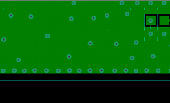
Ground plane always have to be stitched together with vias, round the edges as well is always good, don't need to be so close though, and add some random ones in board, as per picture below. These help break-up any tendency for resonant waves to build up on the planes, more a problem with power ground pairs, but can still effect just ground planes. Stitching vias round the edge of boards (a techniques used in RF design a lot) also helps supress edge radiation of noise.
The above stackup would be great for this design as you get excellent shielding for EMC purposes. Most commercial boards tend to have a hybrid version of this, where there are a mixture of tracks and copper pour on the top, as it limits the number of PTH vias, which can be problematic from a cost and spacing point of view.
HDI PCB designs though, that I do more and more of these days this is coming back into fashion as the vias are laser drilled and only pass through one layer so you don't block inner layer routing directions, also the cost doesn't go up when you start getting into the few thousand vias on a board. We have many a merry discussion on the various board stack-ups that are available for a particular design as there are advantages and problems with all choices. There are so many factors at play it can be quite fun (if you are into PCBs to the same SAD extent I am).
One area where todays high speed boards differ is power planes will have a closely coupled ground planes (both are done as planes, the power is not routed as tracks unless the design is very simple) to give buried capacitance.
http://www.ddmconsulting.com/Design_Guides/bcguide.pdf
Decoupling this is OTT for this design but usefull knowledge as you go on to more complex designs.
No you need the low value 0.1uF next to the pin, for the high frequency decoupling it provides, the rule for the pin decoupling capacitors is actually find the smallest package available for the value chosen...
http://www.pcbcarolina.com/images/01_pcb_power_decoupling_myths_debunked.pdf
Decoupling
Decoupling
http://www.intersil.com/content/dam/Intersil/documents/an13/an1325.pdf
Had a look at the TDA1541 thread, and looking at the data sheet for said device...some thoughts, don't like the star routing much, but it is a bit of a strange device and I have seen numerous solutions, but the decoupling caps do have high frequency noise on them and as such the lowst impedance return path should be used.🙂
Sorry for OT.
Attachments
Eldam: You're saying "use the largest capacitor value within the package size". I've chosen 0805, for practical reasons (my smd soldering experience is limited). So I could actually use 1uF for decoupling instead of 100nF?
I also see that Panasonic has some polymer caps with ESR down to 20 mOhm. That's lower than a lot of film caps even. I'm gonna try these for decoupling as well.
Hi Painkiller,
So do I, I just soldering once smd with the Grup buy Subbu 3 project here at DIYAUDIO. But I liked it, if you can soldering 805, you can with 605 that's my experience, but each time the harder is to avoid the smt cap moving for clean soldering ! I have no longer experience but asking myself for a better technic that the nails ! Maybe a micro drop of glue in the center of the case ? In this project there was 603 case and i succees with the "nails" technic:
Do we are able to hear the difference between 603 and 805 case with those old technologies (it's not CMOS inside the chip ?!) and NOS ?
I use copy&paste from IBM pdf Marce gave us above for the "use larger...."
On Mouser or Digikey it's easy to find the better ESR with the search engine, you can find lower than 20 mohm for 47 uf. but if this value is not limited by the design you can also use 570 uF and find 5/7 mHoms (SEPC/F caps e.g). on the pins o closest to the pins of the chip : 0,1 uF smd X7R/NPO (NPO is in theory better but my understanding is the frequencies involved are below the capacity of both.. so same result here: has to be check, I'm not sure). Notice than if the chip need always this decoupling (if the second pin on the chip is gnd : soldering on the pins if your able to is not bad if you leave enough space to use connector of course as Peufeu showed... so near the plastic body !).
For the Polymers : go for UCC or Panasonic types, they give better subjective result and 2 to 2.5 pitch exist. 0.1 uf WIMA MKT (MKS2 serie) exist with 2.5 pitch (Mouser). For decoupling I give up Silmic 2 for analog and prefer KZ muse (tonal balance is better for me): But use Peufeu's plugs also for testing caps and resistor on your design... especially for the i/v resistor (Rhopoint if you have money 11 euros piece ! wirewound each time)
@ Marce : thank you Marce to had a look on the TDA thread and the pictures of RyanJ. I believe he tooks the design from John ECDESIGNS thread who offers it to DIY communauty. John spend time with measurement but I'm not sure he has your high experience with RF design... For me too as just an enthusiast it seems more logical to use a non star ground just under the chip... maybe those questions of the two ranks of caps need those design, I don't know. Old Marantz are maid like this also (I'll try to take a picture if you put a testimonie on the said thread). I'm sure your advise will help a lot.
- Home
- Source & Line
- Digital Line Level
- AD1862 PCB layout