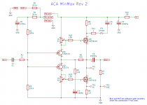
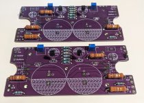
At Burning Amp 2023, @PSz. asked if I would help adapt the ACA mini into the store's ACA chassis, which will greatly increase thermal dissipation, but I think more importantly for Paul, will stack nicely on his other ACAs. I accepted and here we are about a month later with the ACA MinMax.
Please leave your feedback and comments!
Edit 2023/10/31:Rev 0.1 now attached to this post.
Edit 2023/11/02: Ordered boards!Rev 0.2 now attached
Edit 2023/11/09: Bill of materials here. Chassis wiring diagram attached to this post.
Edit 2024/01/08:Rev 1 schematic and boards now attached.
Edit 2024/03/19: Rev 2 schematic and boards now attached.
- PCB holes and transistor locations match store chassis
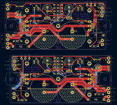
- Right and left PCB layouts to keep wiring clean
- 35mm capacitor footprints for increased voltage rating (50V)
- Compatible with TO-220 or TO-247 output devices
- Optional gate stopper resistors (R12, R13)
Rear switch used for distortion reduction circuit (previously on-board jumpers)- Uses on-board jumpers
- Requires at least a new SPDT front switch, original uses SPST. A DPDT is even better
- XLR input can be used for balanced mono (balanced source required)
- Rear switch can be used for parallel mono
- Markings on the chassis back panel will make no sense
Please leave your feedback and comments!
Edit 2023/10/31:
Edit 2023/11/02: Ordered boards!
Edit 2023/11/09: Bill of materials here. Chassis wiring diagram attached to this post.
Edit 2024/01/08:
Edit 2024/03/19: Rev 2 schematic and boards now attached.
Attachments

Last edited:

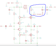
Suggest swapping the positions of C2 and C3. R10 and C3 are a RC filter for the V+ power, and the C3+ terminal is the point of cleanest V+ and the C3- terminal is the clean ground. Keep them close to the board inputs of V+ and GND. Connect R10 directly to C3+ and connect R8 directly to C3+.
@N Brock I like what you did there. I've done something similar with the ACA chassis but did not mirror image the boards or allow for higher voltage supplies or outputs, You have some very nice touches in your design. Well done! I am looking forward to seeing the completion.At Burning Amp 2023, @PSz. asked if I would help adapt the ACA mini into the store's ACA chassis, which will greatly increase thermal dissipation, but I think more importantly for Paul, will stack nicely on his other ACAs. I accepted and here we are about a month later with the ACA MinMax.
When the H2 switch is open, the bottom plate of supercapacitor C6 is disconnected from the rest of the world and is completely floating. If someone closes the switch while the amp is turned on and a speaker is connected, this might cause a bit of a thump while C6 charges or discharges to its correct final bias voltage.
One possible workaround might be to connect a new, high value, bias resistor between C6's bottom plate and the right hand terminal of R11. In other words, in parallel with the switch (!). Set the new resistor to be approx four orders of magnitude (80 dB) bigger than R8; namely, 7.5 Kohms. Now the switch selects between (7501 ohms) and (1.00 ohms) resistance, connected between C6 and Q3source. And C6 bottom plate is always at the correct bias potential, for both positions of the switch, reducing the possibility of a charge/discharge "thump".
Remember though, that if the amp is delivering 1 watt into an 8 ohm load, a signal current of 0.35 amperes flows from the source of Q3 to the positive supply. 57% of this current flows through R8 and 43% of this current flows through R11. That means (0.43 * 0.35) = 150 mA of signal current flows through the (closed) H2 switch, when the amp is delivering 1 watt into an 8 ohm load. Some types of wire (Litz ; microphone coax ; wirewrap wire ; etc) might not be suitable, to connect the two amp channel PCBs to the DPST switch. And some miniature switch types might not be suitable either. For safety, especially when playing the amp LOUD, you probably want wire and a switch rated for a lot more than 150 mA.
Attachments
What a great idea! Subscribed.
🍿
Re: distortion-shaping switch… I suspect this is going to be used only a few times and then each user will decide which configuration to use 99% of the time… it seems that a PC mounted jumper would be completely appropriate.
Ans you’ll want to power down before changing it… which opening the lid will essentially require you to do.
Anyway, my 2¢.
Last edited:
Thank you all for the suggestions!
Rev 0.1
To limit multiple layouts and schematics floating around this thread I'm going to edit the attachments on the first post rather than posting new revs each time.
Rev 0.1
- C2 and C3 are swapped
- Abandoned the rear switch as H2 idea, reverted to an on-board jumper
To limit multiple layouts and schematics floating around this thread I'm going to edit the attachments on the first post rather than posting new revs each time.
I have another suggestion.
I see that the V+ from C3+ goes across the board to the switch pads at the far end of the board, then from the switch up to the top of the board, and then back across the board to P1 located above C3. That is a big loop with a large loop area.
At this point in time you probably don't want to relocate the switch to reduce long route, so my suggestion is to return the V+ from the switch alongside the outgoing trace until it reaches C3+, and then continue up to P1. This will greatly reduce the loop area. And of course tightly twist the wires together from the switch pads to the switch.
Rev 0.2 now up in the first post and boards ordered!
I know PSz and 6L6 are in for this first batch, anyone else interested in building a prototype? Free for anyone who's already commented, all others just pay shipping (~$5 in con. US) and make a soft commitment to build it relatively soon to provide feedback.
I know PSz and 6L6 are in for this first batch, anyone else interested in building a prototype? Free for anyone who's already commented, all others just pay shipping (~$5 in con. US) and make a soft commitment to build it relatively soon to provide feedback.
Thanks Ben, I've now paired up those traces for Rev 0.2 but took a different path along the top of the board. I think it has a similar reduction in loop area compared to your suggested route and has less impact on the rear side ground plane.my suggestion is to return the V+ from the switch alongside the outgoing trace until it reaches C3+, and then continue up to P1
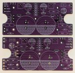
Boards are here 😁 This is my first time trying purple and I'm pleased.
I wrote up a parts list here that probably needs another once over before anyone takes it as gospel.
Digikey struggled to ship my order this week so I don't have parts quite yet, but I'm optimistic that I will be able to build soon.
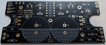
And oops, the silkscreen for the power switch on the right channel gets cut off by the pads. It's on the list for the next rev
I wrote up a parts list here that probably needs another once over before anyone takes it as gospel.
Digikey struggled to ship my order this week so I don't have parts quite yet, but I'm optimistic that I will be able to build soon.
And oops, the silkscreen for the power switch on the right channel gets cut off by the pads. It's on the list for the next rev
Attachments
I'll populate it as soon as I have the parts  Shouldn't be more than a week
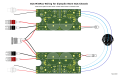
Here's a chassis wiring diagram. I suppose the XLR could be used for balanced sources (I don't have any), and the rear switch for paralleling the inputs, but keeping it simple for now.
Shouldn't be more than a weekHere's a chassis wiring diagram. I suppose the XLR could be used for balanced sources (I don't have any), and the rear switch for paralleling the inputs, but keeping it simple for now.
Attachments
Last edited:
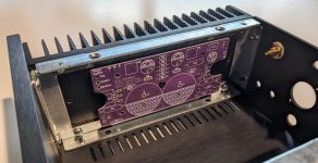
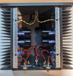
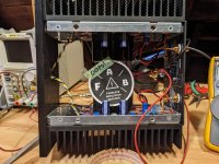
More progress this evening. I've got nearly everything assembled and it's time for first power on and biasing 
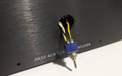
The front power switch I ordered is 22mm diameter, so it doesn't fit in the 20mm hole provided. A substitute DPDT will do for now. Gotta read those datasheets carefully!
I flipped the rear plate around and drilled new holes for the XLR jack.
Wiring is a bit tight in this chassis, so I'd suggest something smaller than the 14 gauge that I used for the power and speaker connections. I'm on the lookout for a DC jack with larger solder terminals as well.
Attachments
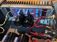
This fearless amp builder may have gotten a bit too fearless.
All pots fully counterclockwise, front switch off
Plugged in 36V 5A SMPS
Observed output protection pulsing behavior, this was somewhat expected as the PSU charges the large caps
Pulsing doesn't stop
Change to my bench supply (I should have used this from the beginning)
Slowly ramp voltage and watch current, not much from zero to 5V, over 5V current climbs and reaches the (arbitrary) 1A current limit at 8.5V
At the SMPS's 36V this current must have been rather large
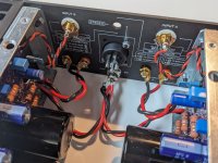
On a single channel, with 6V and 0.22A on the PSU, I measure the following DC voltages (ground ref):
No difference with the switch on or off
Something is wrong, I just don't know what
I don't know if I damaged the MOSFETs when removing them from my original ACA mini, if the NOS JFETs are the culprit, or if there's something wrong with my board layout.
Whichever it is, I think I'll take a little break and resume this weekend.
If anyone has suggestions for in-circuit tests that I could try to narrow things down before I take everything apart, please let me know.
Prototype builders beware!
All pots fully counterclockwise, front switch off
Plugged in 36V 5A SMPS
Observed output protection pulsing behavior, this was somewhat expected as the PSU charges the large caps
Pulsing doesn't stop
Change to my bench supply (I should have used this from the beginning)
Slowly ramp voltage and watch current, not much from zero to 5V, over 5V current climbs and reaches the (arbitrary) 1A current limit at 8.5V
At the SMPS's 36V this current must have been rather large
On a single channel, with 6V and 0.22A on the PSU, I measure the following DC voltages (ground ref):
| Right Channel | Q1 (2SK170) | Q2 (2SJ4) | Q3 (IRF9520) | Q4 (IRF520) |
|---|---|---|---|---|
| Gate | 3.91 | 3.91 | 5.71 | 4.52 |
| Drain | 5.71 | 4.52 | 5.69 | 5.69 |
| Source | 4.56 | 4.56 | 5.75 | 0.16 |
Something is wrong, I just don't know what
I don't know if I damaged the MOSFETs when removing them from my original ACA mini, if the NOS JFETs are the culprit, or if there's something wrong with my board layout.
Whichever it is, I think I'll take a little break and resume this weekend.
If anyone has suggestions for in-circuit tests that I could try to narrow things down before I take everything apart, please let me know.
Prototype builders beware!
Attachments
Some thoughts:
1. 2SK170 2SJ74 pins 1 2 3 are D G S. Your PCB schematic shows pin 1 at the S position and pin 3 at the D position. However the PCB copper traces and silkscreen appear to show correct connections of 2 to 2 and 3 to 3. So despite the schematic, the PCB appears correct.
2. Check setting of trimmer P2. Vgs of Q4 is 4.52V-0.16V=4.36V. See if you can adjust the trimmer so that Vgs is close to zero.
3. Q2 did not drop much voltage from S to D. Perhaps that is due to the trimmer setting or perhaps there is an issue with the JFET. So check it again after adjusting trimmer P2.
4. The gate voltages for Q1 and Q2 appear high. Check R2, R3, R4 for correct resistances.
5. Check the usual things: correct component values and solder joints, correct PCB schematic/circuit.
I don't have anything definitive, but @PSz. build up the boards I sent him and had no issues. So I ordered another essentials kit from the store and will swap out all the transistors  . My bet is that I damaged one (or more!) of the devices while de-soldering. Lesson learned, use known good parts when building prototypes
. My bet is that I damaged one (or more!) of the devices while de-soldering. Lesson learned, use known good parts when building prototypes- Home
- Amplifiers
- Pass Labs
- ACA MinMax - ACA mini retrofit for ACA chassis