
Thank you for your recommendations. I resoldered all solder joints and cleaned the PCB with isopropyl alcohol, still can’t get bias above 4.5dcv. So in review, original build worked totally on both ACA’s and biased OK on all channels. Then, implemented Tungsten’s parts upgrade except for the three electrolytic caps and soldered 1 microfarad polypropylene caps in parallel to all electrolytic caps. 1 amp works perfectly but the other amp has 1 channel that won’t bias- is stuck at 4.6 volts. I backed out all the 1 microfarad ppl caps. Still won’t bias. Verified that all caps were oriented correctly. Resoldered all the connections twice and cleaned the pcb as per suggestion. Still won’t bias. So, just on the outside chance something happened to the caps I inserted the three Tungsten recommended caps into their locations on the board, correctly oriented and powered up- still won’t bias. Changed power brick, no change. Then I saw Allen’s test points for Volts and Ohms on the parts on the PCB. The working channel checks out ok but the bad channel is off on almost, but not all measurement points for both volts and ohms.eg for Volts:Q1 S-.03, D-4.33(should be 12v), G-.75 (sb 4.5), transistor leg-23.91, R10-1.56 (sb 3.8), R9-1.7 (sb 4.5), R15 e 4.31 (sb 11.9), R15C-9.49 (sb 17.5), Q2 G-9.49 (sb17.5), D-23.88 (sb 24), S-5.19 (12.7) For Ohms: Q1S-7.1 ohm (sb 0), D-179 ohm (sb 5.2k), G-64 ohm (sb 1k), R10-334k (sb 335k), R9-131 ohm (sb 1k), R15 e- 179 ohm (sb 5.2k), R15b-876 ohm (sb 5.8k), R15c-10.1k (sb 10.9k), Q2 G-10.2k (sb 11k), D-163 ohm (sb 1k), S-180 ohm (5.2k).
So most measurements are a ways off, but a few are ok. Is this of any help in analyzing the problem? Any additional suggestions. Thanks for your ideas and assistance!
So most measurements are a ways off, but a few are ok. Is this of any help in analyzing the problem? Any additional suggestions. Thanks for your ideas and assistance!
Thank you for your recommendations. I resoldered all solder joints and cleaned the PCB with isopropyl alcohol, still can’t get bias above 4.5dcv. So in review, original build worked totally on both ACA’s and biased OK on all channels. Then, implemented Tungsten’s parts upgrade except for the three electrolytic caps and soldered 1 microfarad polypropylene caps in parallel to all electrolytic caps.
1 amp works perfectly but the other amp has 1 channel that won’t bias- is stuck at 4.6 volts. I backed out all the 1 microfarad ppl caps. Still won’t bias. Verified that all caps were oriented correctly. Resoldered all the connections twice and cleaned the pcb as per suggestion. Still won’t bias. So, just on the outside chance something happened to the caps I inserted the three Tungsten recommended caps into their locations on the board, correctly oriented and powered up- still won’t bias. Changed power brick, no change.
Then I saw Allen’s test points for Volts and Ohms on the parts on the PCB. The working channel checks out ok but the bad channel is off on almost, but not all measurement points for both volts and ohms.eg for Volts:
Q1 S-.03, D-4.33(should be 12v), G-.75 (sb 4.5),
transistor leg-23.91,
R10-1.56 (sb 3.8),
R9-1.7 (sb 4.5),
R15 e 4.31 (sb 11.9), R15C-9.49 (sb 17.5),
Q2 G-9.49 (sb17.5), D-23.88 (sb 24), S-5.19 (12.7)
For Ohms: Q1S-7.1 ohm (sb 0), D-179 ohm (sb 5.2k), G-64 ohm (sb 1k),
R10-334k (sb 335k),
R9-131 ohm (sb 1k),
R15 e- 179 ohm (sb 5.2k), R15b-876 ohm (sb 5.8k), R15c-10.1k (sb 10.9k),
Q2 G-10.2k (sb 11k), D-163 ohm (sb 1k), S-180 ohm (5.2k).
So most measurements are a ways off, but a few are ok. Is this of any help in analyzing the problem? Any additional suggestions. Thanks for your ideas and assistance!
I couldn't comprehend your post as it is one massive run-on paragraph so I did some editing.
First thing, you said that you can't get the bias to 12V. I assume you mean you can't get the drain voltage of Q1 up to 12V.
The voltage at R9 and at Q1 gate should be the same, as R9 is connected to the Q1 gate through an 100R resistor, and the gate current should be very small.
Your big issue is 1.7V at R9. Is this the highest voltage that you can get with the pot set at maximum? This is Q1 gate voltage/JFET source voltage.
What is the voltage at R10 relative to Ground? This is the JFET gate voltage. Is it 4.33V, which is also Q1 drain voltage as they are connected if the pot is maxed out.
Another thing to check out is R9. Lift one leg to take it out of the circuit and measure its resistance. Is it 1k?
Thanks for getting back to me Ben Mah and also for fixing my massive run-on sentence. Ok, for grins this morning I swapped the boards to the opposite sides of the chassis, in case I had a bad solder or broken wire on the power supply wire. I show 24v dc at the board/wire connection and still have 1 bad board. Your measurements request on the bad board are:
Q1 middle pin- 5.14vdc
R9- .01v dc (outside leg) and 3.86vdc (inside leg- closest to middle of the board)
R10- 5.2vdc (outside leg) and 4.11vdc (inside leg)
disconnected from the circuit R9 reads 1k (997ohm)
pot set at maximum and most of the voltage numbers continued to bounce around within a narrow range.
thanks
Your R9 voltage is now different. It was 1.7V and now it is 3.86V. Perhaps the pot was not at its maximum previously?
The voltage drop across R10 is quite high. There appears to be too much current flowing through it. The voltage at both sides of R10 should be about the same. So either the JFET is bad or the input capacitor is bad. Check the input RCA jack for voltage at the centre pin relative to ground. If the input capacitor is working properly there should be no DC voltage at the input. So if the capacitor is ok, then the JFET is likely bad.
The voltage drop across R10 is quite high. There appears to be too much current flowing through it. The voltage at both sides of R10 should be about the same. So either the JFET is bad or the input capacitor is bad. Check the input RCA jack for voltage at the centre pin relative to ground. If the input capacitor is working properly there should be no DC voltage at the input. So if the capacitor is ok, then the JFET is likely bad.
Hi Ben Mah- yes, I believe the pot was not consistent between the measurements.
I tested the rca inputs at the center pin and neither has any dc voltage, therefore itmust be a bad jfet transistor. Thank you for you guidance. Should I get a single jfet or replace the pair?
I tested the rca inputs at the center pin and neither has any dc voltage, therefore itmust be a bad jfet transistor. Thank you for you guidance. Should I get a single jfet or replace the pair?
I would just replace the single jfet. The other channel works so don't fix it if it ain't broke. 🙂
You could buy a pair and keep the other one as a spare.
You could buy a pair and keep the other one as a spare.
https://www.diyaudio.com/community/threads/aca-amp-with-premium-parts.328357/post-7322029
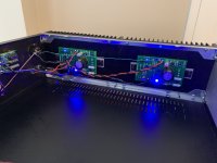
Way to go! Which chassis is that, and what are the little PCBs?
Way to go! Which chassis is that, and what are the little PCBs?
Dual parallel monoblock ACAs to reside in a single 4U full width chassis with substitute UMS heatsinks. Discovered the factory mounting drill / tap layout does not accommodate direct screw in installation of ACA PCBs. Boards mount from supplied standoffs with their corner eyelets (not the center eyelet as in the stock ACA chassis). I need to drill and tap 8 mount holes for the MOSFETS. M3x0.5.

I'm really interested to hear about the differences that you hear when you move to a LPS, I have my ACA running at 36v with dual mono SMPS, way too hot for the original chassis so would really love to move to a larger chassis, and build a power supply. Excited to see how yours turns out!
@Zamjazz27 - understand your concern, my stereo ACA at dual 24v SMPS runs hot, so yours hotter I get that. This morning Keratherms arrived from the DIY store so the PCBs are mounted to the sinks. Now I need confirmation my LPS schematic is correct, then finish wiring bring the amp(s) up and report back to you
It looks like the basic schematic and layout should work.
I probably would have chosen different capacitors for the final bank, but if old computer grade caps are what you have, they are worth a try.
My preferred caps are Kemet ALS series screw terminal for wiring point to point.
I probably would have chosen different capacitors for the final bank, but if old computer grade caps are what you have, they are worth a try.
My preferred caps are Kemet ALS series screw terminal for wiring point to point.
Those little PCBs are the POSZ filter boards from DIY Audio Store, originally designed by Mark Johnson.https://www.diyaudio.com/community/threads/aca-amp-with-premium-parts.328357/post-7322029
Way to go! Which chassis is that, and what are the little PCBs?
I do like the mounting concept-as as there is no baseplate to mount the PCBs.
Thanks Tungsten. Solid copy on your advice. Accordingly I've changed around the order of caps, placed the computer grade adjacent to the bridge, and the Nippon Chemi Con will be last in the chain feeding the PCBs.It looks like the basic schematic and layout should work.
I probably would have chosen different capacitors for the final bank, but if old computer grade caps are what you have, they are worth a try.
My preferred caps are Kemet ALS series screw terminal for wiring point to point.
- Home
- Amplifiers
- Pass Labs
- ACA amp with premium parts