With reference to my post #1,530 last week, I'm beginning to wonder if it is foolish of me to worry about whether or not thermal feedback with bias transistor Q8 is bettered by placement midway between the NPN and PNP output device rows. Looking at a couple of photos of successful implementations of this amp (for example, one using a HiFiOcean board) , I see the Q8 device mounted smack in the middle of the row of NPN output Qs at the top of the circuit board---a half inch from these, and not at all close to the complementary row of PNP output Qs below the circuit board. Plus, when I look at the specification sheets for the MJ11016G (NPN) and Mj11015G (PNP) devices I plan to use, they appear to have the same thermal characteristics.
Given that placement of Q8 on the main heatsink between the two TO-3 device-holding brackets (see photo below), is not terribly close to any output Qs, and is harder to mechanically assemble, maybe I should just locate Q8 on one of these brackets (see other photo below) and assume temperatures at that point are a good proxy for the whole output stage.
Does anyone care to offer an opinion? Or even better--has anyone taken any temperature measurements on a functioning AB100 that might inform the decision. (Mine is a ways from completion).
I believe the closer you are to the transistor, the better Q8 can respond. I haven't seen how anyone else using TO-3 devices solved this issue. My Q8 is mounted right between the two rows, but I'm not using TO-3's. Someone further back in the thread used TO-3's, you might find that and ask him.
Thanks for the feedback, RickRay ! I suspect you are right about closeness to the output transistor resulting in better response from Q8. It stands to reason that heat takes a while to travel through the metal.
Osscar used TO-3 devices in his AB100, but in photos it appears that he had the Q8 mounted very close to a pair of them (I think a complementary pair,, although it's not clear from the photos) which he was able to do by using relatively long wires to connect these output devices to his custom-designed boards.
Osscar used TO-3 devices in his AB100, but in photos it appears that he had the Q8 mounted very close to a pair of them (I think a complementary pair,, although it's not clear from the photos) which he was able to do by using relatively long wires to connect these output devices to his custom-designed boards.

Just starting to load my AB100 pcb's (NP layout), can I ask the other members here who have built this amp and have it running:
1. What position should the 5K bias trimpot P1 be set to at start?
2. Did you adjust the bias as recommended by NP in post #1 to 80mA per rail = 20mA per output device?
3. If not, what bias current per device did you settle on?
4. What DC supply rails are you using?
5. What part number did you use for Q8 - attached to heat sink?
I have had a quick scan of this thread, but can't find much info re biasing.
Many thanks for any replies.
Hi,
yes I mounted next to one pair, but there was a reason for that - because there was already a hole in the heatsink 😀
But overall I think it doesn't matter that much - especially considering that the quiescent current of individual MJ TO3 darlington transistors is quite accurate when measured in Re, so they will heat up similarly.
Also, the thermal mass of the radiator must be taken into account and bias should be adjusted slowly - because radiators heat very little and slowly.
1. Maximum resistance on P1 at the beginning.Just starting to load my AB100 pcb's (NP layout), can I ask the other members here who have built this amp and have it running:
1. What position should the 5K bias trimpot P1 be set to at start?
2. Did you adjust the bias as recommended by NP in post #1 to 80mA per rail = 20mA per output device?
3. If not, what bias current per device did you settle on?
4. What DC supply rails are you using?
5. What part number did you use for Q8 - attached to heat sink?
I have had a quick scan of this thread, but can't find much info re biasing.
Many thanks for any replies.
2-3. At Re=1R and TIP142/147 I would start with the recommended 20mA / transistor. The sweet spot might be a little higher but if you set the bias too high, a potential thermal runaway can occur and kill the output stage. If you adjust it above 20mA, do it slowly, as osscar suggests, with the lid on. It is practically a full Sunday procedure for the background.
4. I decided for +/-50V but already regret it. I would rather choose +/-40V now. The originally nominated transistor types are either very close to or even beyond their factory specified safety margin at +/-50V. For the peace of my mind I settled to different types.
5. Any npn with the compatible pin configuration, which exhibits higher dc current gain at higher temperatures in the relevant Ic range (most of them do).
Many thanks to RickRay, to mcsantos, and to osscar for this valuable practical advice, which will greatly help with the fear factor when I finally crank up the variac to bring my beast to life and start the bias setting procedure! (My wife tells people that I build amps and other audio gear for a hobby, and that I'm "always a little bit surprised when they work". It's never the design that worries me; it's my implementation!)
One of these days I will actually do a layout for this beast, as I have a Dissipante 3U enclosure, and I haven't even opened the box it came in yet. It'll be interesting to see if I can cram everything in place on the 3U-size heat sink. Unfortunately, the layout will most decidedly NOT conform to standard protocol.
For the future builder of the AB100 amplifier, I have a toroidal transformer for sale, we can even agree on the price 🙂
Happy building
New unused, for sale...
AC PRI: 240V
AC SEC: 4x 30V
500VA
Suitable for dual mono stereo amplifier. (41V DC)
The price I paid was 124€, I will sell to a future buyer for 100€ + shipping, ideal inside EU
Wire transfer or PayPal.
AC PRI: 240V
AC SEC: 4x 30V
500VA
Suitable for dual mono stereo amplifier. (41V DC)
The price I paid was 124€, I will sell to a future buyer for 100€ + shipping, ideal inside EU
Wire transfer or PayPal.
Happy building
I've been distracted from working on my AB100 for more than a month, but I'm back on the job. I decided to use newer transistors for Q1, Q2, and Q4 (NPN), and Q7 (PNP) that differ from the original devices specified in the Pass design. This decision has necessitated a slight workaround.
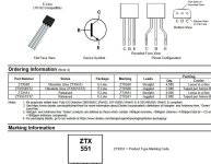
The original Qs called for in the Pass design were ZTX 450 (for the NPN devices), and ZTX 550 (for the PNP device). (Nelson's Q8 was also a ZTX 450, but I'm using a TTC004B there for the bias adjustment circuitry).
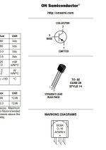
I'm replacing the (NPN) ZTX 450 devices with Onsemi BC63916 devices (easily available and higher voltage rating); and replacing the (PNP) ZTX550 device with Onsemi BC640TA (for the same reasons).
When I double-checked the pinout for all of these Qs, however, I discovered a problem . Facing the flat side of both the ZTX 450 and the ZTX 550, the pinout shown on those devices' datasheets is: (left to right) Pin 1-Emitter; Pin 2-Base, Pin-3-Collector. However, the data sheets for both the BC639 and the BC640 replacement devices, reveal that these devices, again facing the flat side, have a pinout of: (left to right) Pin 1-Emitter, Pin-2 Collector, Pin 3-Base. In short, the Base and Collector leads are reversed in the newer devices.
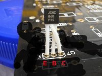
In order to use the newer devices, I twisted the Base and Collector leads, as shown in the attached photograph of a BC640 in the Q7 spot. And then inserted the transistors so that the Emitter lead position agrees with the Pass board silkscreen "E" marking. I checked these revised lead positions against the original Pass schematic, and against the visible PC board tracks, and it seemed like the BC640 would make the right connections with this change. I made the same changes for the BC639 devices for Q1,Q2, and Q4. I have not soldered anything into place yet.
I hope this makes sense and is all correct. I would be interested to know how any other forum members using the BC 639 and BC 640 devices dealt with this problem. I believe member jwjarch included these newer substitute devices in his BOM (attached to post #748), but I don't know any implementation details for his amp.

To prevent shorts resulting from the twisted Q leads, I used some Teflon insulation pulled off of 22 gauge solid-conductor hook-up wire I use for point-to-point perf board. It's thin walled, and not as stiff or bulky as shrink tubing.
The original Qs called for in the Pass design were ZTX 450 (for the NPN devices), and ZTX 550 (for the PNP device). (Nelson's Q8 was also a ZTX 450, but I'm using a TTC004B there for the bias adjustment circuitry).
I'm replacing the (NPN) ZTX 450 devices with Onsemi BC63916 devices (easily available and higher voltage rating); and replacing the (PNP) ZTX550 device with Onsemi BC640TA (for the same reasons).
When I double-checked the pinout for all of these Qs, however, I discovered a problem . Facing the flat side of both the ZTX 450 and the ZTX 550, the pinout shown on those devices' datasheets is: (left to right) Pin 1-Emitter; Pin 2-Base, Pin-3-Collector. However, the data sheets for both the BC639 and the BC640 replacement devices, reveal that these devices, again facing the flat side, have a pinout of: (left to right) Pin 1-Emitter, Pin-2 Collector, Pin 3-Base. In short, the Base and Collector leads are reversed in the newer devices.
In order to use the newer devices, I twisted the Base and Collector leads, as shown in the attached photograph of a BC640 in the Q7 spot. And then inserted the transistors so that the Emitter lead position agrees with the Pass board silkscreen "E" marking. I checked these revised lead positions against the original Pass schematic, and against the visible PC board tracks, and it seemed like the BC640 would make the right connections with this change. I made the same changes for the BC639 devices for Q1,Q2, and Q4. I have not soldered anything into place yet.
I hope this makes sense and is all correct. I would be interested to know how any other forum members using the BC 639 and BC 640 devices dealt with this problem. I believe member jwjarch included these newer substitute devices in his BOM (attached to post #748), but I don't know any implementation details for his amp.
To prevent shorts resulting from the twisted Q leads, I used some Teflon insulation pulled off of 22 gauge solid-conductor hook-up wire I use for point-to-point perf board. It's thin walled, and not as stiff or bulky as shrink tubing.
Link the board and schematic you are using.I'm back on the job
Thanks for your response STOXX. The schematic is contained in Post #1 by Nelson:
https://www.diyaudio.com/community/attachments/ab100-001-gif.323061/
Another, "clarified" version of this same schematic appears in Post #123 by Goat Guy. The clarifications refer to how resistance values are stated, and where crossed schematic lines do or do not constitute a connection.
https://www.diyaudio.com/community/attachments/npassab100-png.348170/
A drawing of the parts layout for Nelson's board appears in his Post # 463, along with the Gerber files. (These are the files I had my boards made from.)
https://www.diyaudio.com/community/attachments/ab100-redux-gif.759301/
https://www.diyaudio.com/community/attachments/ab100-redux-zip.759300/
Beyond the photos I have posted to show stages of construction in my amp, I don't think a photo of either the silkscreen or the back back of the board is contained in this forum thread (not a legible one anyway). Post #491 by rookakoma shows a sort of blurry rendition of both on a pcb order he apparently made to a board fabricator, but I would guess he posted them to give us information on the fabricator he chose, not to guide detailed circuit examination.
https://www.diyaudio.com/community/attachments/ab100_jlc-png.760132/
I will try to get a clear photo of the front and back of one of the blank boards I have and post it tomorrow. Since the board is black it can be tough to see the traces through the protection layer.
Sorry to have such poor evidence to offer you in the above!
Thanks again for your response.
I am going to make a general criticism.response.
Zapped, you are highly likely to make errors in your project.
Send pics of everything to DIAYAUDIO.COM. Just as you are doing.
Fact-check it all. I don't want to insult you but you may have a visual impairment/reading disorder.
You remind me too much of myself.
They are, as far as i can see i your screen shots.No twisty legs are required.
Ztx: CBE (center base)
Bc: ECB (center collector)
- Home
- Amplifiers
- Pass Labs
- AB100 Class AB Power Amplifier