Dear Anand,
I only re-invented the wheel. Attached is the schematic of my already shared board layout.
I think an important aspect (according to D. Shelf) is the ground return of the decoupling modules. He says they should be exclusive and connect to the capacitor ground of the PSU rather than to the star GND.
Having those cap multipliers (and including the active rectification), I measured 80mVpp ripple at the output stage (unloaded amplifier, 50mA/darlington bias - before the thermal runaway accident mentioned above) and 5mVpp ripple after the cap multipliers. The latter seemed to be very satisfying to me.
Another potential issue is that - unlike the simple RC decoupling - the transistors in the +/- rail cap multipliers may wake up with a slightly different time-delay, causing a turn-on thump. In my case, I am not concerned about this because the speaker relay circuit, which is powered from the positive rail of the output stage, is designed to wake up with a 3-4 sec delay, long after any thump has been unleashed.

Best,
Miklos
I only re-invented the wheel. Attached is the schematic of my already shared board layout.
I think an important aspect (according to D. Shelf) is the ground return of the decoupling modules. He says they should be exclusive and connect to the capacitor ground of the PSU rather than to the star GND.
Having those cap multipliers (and including the active rectification), I measured 80mVpp ripple at the output stage (unloaded amplifier, 50mA/darlington bias - before the thermal runaway accident mentioned above) and 5mVpp ripple after the cap multipliers. The latter seemed to be very satisfying to me.
Another potential issue is that - unlike the simple RC decoupling - the transistors in the +/- rail cap multipliers may wake up with a slightly different time-delay, causing a turn-on thump. In my case, I am not concerned about this because the speaker relay circuit, which is powered from the positive rail of the output stage, is designed to wake up with a 3-4 sec delay, long after any thump has been unleashed.
Best,
Miklos

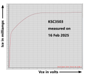
In my experience, KSC3503 and KSA1381 perform quite poorly as capacitance multiplier pass transistors, especially when the current exceeds 5 mA. These are high voltage devices and, unfortunately, it turns out their performance at low Vce is terrible. As you know, capacitance multipliers operate at very low Vce, often less than a volt. In the schematic of post #1,541 the capacitance multiplier devices Q9 and Q20 are KSC3503 and KSA1381. Their performance will suffer.
I estimate that the capacitance multiplier circuits in #1,541 are conducting approx. 12-14 milliamps -- about 4 mA in the first differential stage and about 8-10 mA in the second VAS stage.
So I dug around in my parts cabinet just now and found a KSC3503, which was promptly inserted into the curve tracer's ZIF socket. Measured results are attached below. (The phenomenon on this graph is called "quasi saturation" and many, but not all, high voltage transistors suffer from it. A famous example, which bit Douglas Self in the assz, is the MPSA42 / MPSA92 pair; their quasi saturation is stunningly awful). In the hybrid-pi small signal model of BJT operation, the "ro" parameter drops like a stone when quasi saturation kicks in at low Vce.
The transistor plotted below doesn't really perform well until its Vce exceeds about 4.0 to 4.5 volts. And it's terrible -- it ceases to isolate the ripple input (@ collector) from the clean output (@ emitter) -- at Vce = 1 volt where the circuit of post #1,541 will operate.
This is one reason why I chose to build the capacitance multipliers on my little "Yes It Will Drive an F4" front end card (link) using different devices and not C3503/A1381 . I measured a whole bunch of candidate transistors and chose devices with no quasi saturation. These capmul filters give about 40-50dB (100-300x) of ripple rejection at 120Hz. Other designers will make other choices of course.
_
Attachments
Thanks for your analysis. What I had in mind when I chose Q19 and Q20 is that they must survive 50V Vce. Although the Vce voltage drop during steady state operation is less than 1V, during the turn-on transient I expect it to be higher. And the KSC/KSA were already at hand. Again, I measured that the 80mVpp ripple before the multiplier was reduced to 5mVpp after it. On top of the +/-49.3V front-end rails I found this quite satisfactory. Other time-dependent power fluctuations coming from the mains can easily override this, right?
Nevertheless, if you propose a specific alternative (ECB pins preferred), I am more than happy to swap to them and see how they outperform the KSC/KSA. In your linked circuit I see MJE340/350. Did you mean those? They look like 300V devices and the saturation voltage is unfortunately not given in their datasheet.
Nevertheless, if you propose a specific alternative (ECB pins preferred), I am more than happy to swap to them and see how they outperform the KSC/KSA. In your linked circuit I see MJE340/350. Did you mean those? They look like 300V devices and the saturation voltage is unfortunately not given in their datasheet.
If you're happy with 80mV input ---> 5mV output (16x attenuation), then you're happy. No need to pursue 100x or 300x attenuation when you're happy with 16x.
You might enjoy testing your LTSPICE model to see whether it does or does not match the measured data in post #1,542 above. Here's what I see when I simulate using the KSC3503 transistor .MODEL found on Bob Cordell's spice model page (link). It's very clear that Bob's .MODEL does not include the quasi saturation observed on real devices.
_
Attachments
It is clear without simulation that the lower the saturation voltage the better and so is higher 100Hz damping. Any advice of yours toward these merits are highly appreciated. Furthermore, device models in LTSpice may or may not be real, as you just pointed out. I assume you measured the MJE340/350 saturation behavior before you decided for them in your front-end design linked above. Can you share the corresponding experimental data?
I also wonder what conditions your curve tracer applied in the figure of #1542. What I measure on the KSC is indeed Ic=12mA and Vce=0.8V, exactly as you estimated in #1542. I am a little confused, because this point is considerably off from your trace.
I also wonder what conditions your curve tracer applied in the figure of #1542. What I measure on the KSC is indeed Ic=12mA and Vce=0.8V, exactly as you estimated in #1542. I am a little confused, because this point is considerably off from your trace.
I just completed the following breadboard experiment.
As for the DC part, I get the expected 0.7-0.8V difference between collector and emitter. As for the AC part, I attach below the scope screen-shots. Surprisingly, all transistors seem to attenuate the 800mVpp ripple to 12mVpp. A factor of 66.
Where am I fooling myself...? I tried to find some information about the input impedance of my Siglent scope in AC coupling mode but the manual does not state it. Leaving LTSpice behind, how would you measure the ripple rejection of the cap multiplier?


- Assembly: the positive rail decoupler of #1541 and a load resistor corresponding to 12mAdc.
- AWG output: 4Vdc + 0.8Vpp/100Hz sinus (the AWG certainly cannot provide 50V offset and I do not have an AC-DC mixer at home).
- Measured: 2-CH scope, AC coupling, input and output ripples.
- Transistors tested: KSC3503, MJE340G, TTC004B.
As for the DC part, I get the expected 0.7-0.8V difference between collector and emitter. As for the AC part, I attach below the scope screen-shots. Surprisingly, all transistors seem to attenuate the 800mVpp ripple to 12mVpp. A factor of 66.
Where am I fooling myself...? I tried to find some information about the input impedance of my Siglent scope in AC coupling mode but the manual does not state it. Leaving LTSpice behind, how would you measure the ripple rejection of the cap multiplier?
OK, I probably found it: 66x attenuation corresponds to 36.4dB. The scope manual says channel isolation >40dB. They are not very far...It is getting late in Europe but sometimes next week I will repeat the measurements with one channel only. The yellow input I know anyhow.
Until then, thanks again for the heads-up, Mark. The cap multiplier is clearly a spot with room for optimization.
Until then, thanks again for the heads-up, Mark. The cap multiplier is clearly a spot with room for optimization.
Last edited:
Please allow me to stay with the cap multiplier topic for another post or two. I would also be pleased to know an expert opinion as opposed to my potentially naïve reasoning.
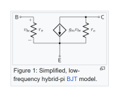
I did another breadboard experiment, see the layout in figure 1. This is essentially the cap multiplier module without the capacitors. The voltage source was an AWG swept between 0-3V at 10Hz. I used two scope channels to measure (i) this output voltage and (ii) Vce. The latter is a direct measurement, whereas the current can be calculated as (V1-V2)/100R.

I tested 3 transistors in place of the npn; KSC3503, MJE340 and TTC004B. I wanted to see their low-frequency saturation behavior, whose importance was pointed out by Mark. Figure 2 shows the results (forgive me for the ugly quantization noise which I was too lazy to smooth out, I really only have the cheap 8-bit DSO at home, but the message is still clear).

This figure made me conclude how I used to misunderstand the operation of such a capacitance multiplier. Previously, I thought that the lower the Vce saturation voltage and the flatter the Ic(Vce) trace is the better. Why? Because then shaking the Vce due to 100 Hz ripple noise before the multiplier will not result in any shake in the current, right?
Only, looking at Figure 2 there is no saturation at all at 12mA. Why? Because all those Ic(Vce) traces given in the transistor datasheets are provided at constant Ib values. Which is by far not the case in our little circuit: In our case Ib is provided from the collector through the 470R resistor. It is not expected to be constant at all, as Vce changes. Consequently, the measured traces are still rising steeply where the 12mA horizontal line intersects.
So what is really the mechanism of the ripple rejection here, if not the nice horizontal transfer curve of the npn? Simply the fact that adding the 220uF capacitor between base and ground, we create a 1/(2*pi*100Hz) = 7.23 Ohm path for the 100Hz current component toward ground which is a much lower resistance path than its sole alternative through the transistor base. In contrast, the dc component of the current sees the capacitor as an open circuit, so this contribution must go through the transistor base and nowhere else.
In the end, ripple rejection happens because only a tiny fraction of the ac current can make it through the base. This tiny fraction would still ‘shake’ Ic a little bit after the multiplier but by far not as much as before it. In this respect, the lower hFE high-voltage transistors may even be beneficial. In the extent of shaking, the slope of the Ic(Vce) trace still plays a role, of course. Quite counter-intuitively, though, this slope is actually the lowest for the incriminated KSC. The only price for this is is a little higher voltage drop across the transistor (0.8V for the KSC, 0.7V and 0.65V volt for the MJE and TT, respectively.)
p.s. Sunday evening I was puzzled why my published ripple rejection breadboard measurements did not show any difference for the three very different npn characteristics. I almost accused my poor scope for above-specs channel-crosstalk. Forgive me, my friend… 😉 Now it is all clear. The RC filter around the base plays the key role here. The effect of the npn type is less pronounced.
Mark, please let me know if you spot an error in my measurements / reasoning / conclusions.
All the best (and thanks for reading through),
Miklos
I did another breadboard experiment, see the layout in figure 1. This is essentially the cap multiplier module without the capacitors. The voltage source was an AWG swept between 0-3V at 10Hz. I used two scope channels to measure (i) this output voltage and (ii) Vce. The latter is a direct measurement, whereas the current can be calculated as (V1-V2)/100R.
I tested 3 transistors in place of the npn; KSC3503, MJE340 and TTC004B. I wanted to see their low-frequency saturation behavior, whose importance was pointed out by Mark. Figure 2 shows the results (forgive me for the ugly quantization noise which I was too lazy to smooth out, I really only have the cheap 8-bit DSO at home, but the message is still clear).
This figure made me conclude how I used to misunderstand the operation of such a capacitance multiplier. Previously, I thought that the lower the Vce saturation voltage and the flatter the Ic(Vce) trace is the better. Why? Because then shaking the Vce due to 100 Hz ripple noise before the multiplier will not result in any shake in the current, right?
Only, looking at Figure 2 there is no saturation at all at 12mA. Why? Because all those Ic(Vce) traces given in the transistor datasheets are provided at constant Ib values. Which is by far not the case in our little circuit: In our case Ib is provided from the collector through the 470R resistor. It is not expected to be constant at all, as Vce changes. Consequently, the measured traces are still rising steeply where the 12mA horizontal line intersects.
So what is really the mechanism of the ripple rejection here, if not the nice horizontal transfer curve of the npn? Simply the fact that adding the 220uF capacitor between base and ground, we create a 1/(2*pi*100Hz) = 7.23 Ohm path for the 100Hz current component toward ground which is a much lower resistance path than its sole alternative through the transistor base. In contrast, the dc component of the current sees the capacitor as an open circuit, so this contribution must go through the transistor base and nowhere else.
In the end, ripple rejection happens because only a tiny fraction of the ac current can make it through the base. This tiny fraction would still ‘shake’ Ic a little bit after the multiplier but by far not as much as before it. In this respect, the lower hFE high-voltage transistors may even be beneficial. In the extent of shaking, the slope of the Ic(Vce) trace still plays a role, of course. Quite counter-intuitively, though, this slope is actually the lowest for the incriminated KSC. The only price for this is is a little higher voltage drop across the transistor (0.8V for the KSC, 0.7V and 0.65V volt for the MJE and TT, respectively.)
p.s. Sunday evening I was puzzled why my published ripple rejection breadboard measurements did not show any difference for the three very different npn characteristics. I almost accused my poor scope for above-specs channel-crosstalk. Forgive me, my friend… 😉 Now it is all clear. The RC filter around the base plays the key role here. The effect of the npn type is less pronounced.
Mark, please let me know if you spot an error in my measurements / reasoning / conclusions.
All the best (and thanks for reading through),
Miklos
Last edited:
The hybrid-pi parameter "ro" is the quantity of interest, since it is a resistor which connects collector to emitter in small signal analysis. AC signals on the collector (the raw DC input to the capacitance multiplier) are sent to the emitter (the "smoothed" DC output from the capacitance multiplier) through ro. In small signal analysis, its resistance is equal to dVce/dIce -- the reciprocal of the slope of the collector current curve.
Notice that ro has nothing to do with the base voltage; it's just 1/(the slope) of the particular I-V curve of the specific transistor, which varies with the wafer fab manufacturing process. ro is not set by The Almighty, it's set by a bunch of engineers and fab technicians at Fairchild.
In capacitance multiplier circuits, ro forms the top half of a (small signal) voltage divider circuit. The bottom half is the input impedance of whatever circuitry is driven by the capacitance multiplier. Usually that input impedance is pretty high, which means most of the noise on the capmul input is transferred to the capmul output. The voltage divider equation is: vout/vin = (Z_load_on_capmul)/(Z_load_on_capmul + ro) . Since ro is small, vout/vin is high. Noise on the collector is transferred to the emitter. Regrettably. If somehow you could make ro become huge, then vout/vin would become tiny, and that would be very desirable.
If you want to measure ro for three different transistor types, set up your curve tracer to apply Vce=0.80 volts and sweep Ice from 10mA to 15mA. Then ro is 1/(the slope of this curve at Ice = 12mA) . You seek a transistor with as high an ro as possible, at the operating point expected in the final gear.
_
Attachments
Dear Mark,
thank you for your quick and clear reply.
I agree with your analysis relying on the Ice(Vce) slope and the voltage divider effect. However, in my opinion the slope of the Ice(Vce) trace must be evaluated by taking the actual potential/current at all 3 transistor terminals into account at the operation point of the application.
So in practice: among all candidate transistors one should seek the smallest slope around the relevant Vce and Ice values (0.8V, 12mA, in my example) but also at the realistic Ib value. This means that the relevant Ice(Vce) trace in our application is not the one measured at constant Ib (e.g. the attachments in #1542 and #1544) but the (very different) one measured in the presence of the 470 Ohm connecting the collector and the base (e.g. #1548). It is unexpected also to me, but in the latter figure the KSC displayes the smallest slope at the operation point.
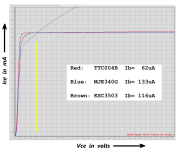
Mark, you insist on the constant Ib throughout the Vce sweep. This is where I disagree with you. In the cap multiplier application the base is tied to the collector via a relatively low, 470 Ohm resistor. This makes a drastic difference in the Vce sweep. For measuring or modeling the Ice(Vce) transfer characteristic, which is directly relevant for our application, this resistor must be included. If you do so, you will get the traces in my experimental Figure 2 under #1548. There, the lowest slope corresponds to the KSC5303.
I think you've forgotten that ro is a small signal resistance whose value is independent of small signal vbe.
I also think you've forgotten that you observe a vout/vin ratio of 1-to-16 with a real KSC3503 which exhibits real quasi saturation, while other capacitance multipliers using different transistors with no quasi saturation, get vout/vin ratios of 1-to-100 up to 1-to-300.
I also think you've forgotten that you observe a vout/vin ratio of 1-to-16 with a real KSC3503 which exhibits real quasi saturation, while other capacitance multipliers using different transistors with no quasi saturation, get vout/vin ratios of 1-to-100 up to 1-to-300.
Let me re-phrase it: We have a 'box' called 'cap multiplier' sitting in our rail. It consists of a transistor, a resistor and a capacitor. For the sake of the dc analysis we can momentarily forget about the capacitor. So we want to deduce the dc transfer function of this box, consisting of the transistor AND the resistor: what voltage across the box gives us what current. If this current-voltage relation is flat, we are happy, because then we can expect more ripple rejection.
I do not deny the usefulness of knowing the Ice(Vce) @ Ib = constant relation of the transistor alone. My point is that, at the end of the day, this is not what we ultimately need but the same relation for the entire {transistor + 470 Ohm} combo, where the Ib = constant boundary condition clearly does not apply during the Vce sweep.
Please note that the above approach does not rely on the validity of any model assumptions.
As you cite my previous post correctly, using the KSC3503 in the cap multiplier, I measured a 16-fold attenuation for the 100 Hz ripple in the amplifier with a biased output stage. In contrast, I measured a factor of 66-fold attenuation in the breadboard test with the same transistor type. This is indeed a significant difference which I attribute to the "cleaner" environment in the breadboard experiment: in the latter I used a clean, regulated lab supply and all current and voltage levels were reasonably low. In contrast, in the running power amp I had a whole zoo of sources for 100 Hz pickup nearby, even after the cap multiplier. Therefore it was difficult to say which part of the 100 Hz was attenuated from the OS rail and which was re-contamination.
To sort this out experimentally, I will definitely replace the KSC/KSA transistors in my cap multipliers with the TTC/TTA's (as they measured the best for you) and report here the attenuation values. Until then, may I ask you to share where exactly your 300-fold 100 Hz (or 120 Hz) ripple attenuation comes from? Simulation? Breadboard measurement? Measurement in a real amplifier environment (if so, what rail voltage and what load on the connecting OS rails)? The latter would be very impressive.
Thank you in advance,
Best,
Miklos
I did the following LTSpice simulations.
I picked some random npn-s from the standard Spice library: some with low saturation voltages and one with no saturation at the voltage range of interest. Black: 2N5550, red: BC547B, blue: BC547C, green: 2SCR375P.
The solid lines in Figure 1 show the Ice(Vce) relations at constant Ib for the transistors only. The dashed lines show the Ice(Vce) relations of the same transistors, when their base is tied to their collector by 470 Ohm.
Figure 2 shows the attenuation of the positive rail cap multiplier at Vc=50V and Ice = 12mA. The RC filter consists of 470 Ohm and 220uF, as in my amp layout.
Conclusions:
- The attenuation at 100 Hz is largely insensitive to the transistor type. It is -36.25 dB for the 3 'saturating' transistors and -35.66 dB for the 'non-saturating' transistor. These dB values translate to 65-fold and 60-fold attenuation, respectively. Remember, on Sunday I measured the very same attenuation for the KSC3503, MJE340 and TTC004B on the breadboard, which left me with scratching my head back then. Now it makes perfect sense: it is really not the transistor but the RC filter, as I reconsidered earlier this week.
- The attenuation gets significantly better above 100 Hz for the saturating transistor types. So Mark's suggestion of using low saturation voltage transistors is good.
So how do we achieve a 300-fold attenuation at 100 Hz, then? Playing with R and C revealed that at 470 Ohm / 1000uF the 100 Hz attenuation is around -50dB for the saturating transistors, which is right there: 316. The questions are if we really want to use such an extreme large capacitor in that position? And does it make sense at all to fight the front-end rail voltage ripple below a few millivolts, when the ground lines will anyhow pick up this much amount of voltage fluctuations?
I don't have too much to add other than if you happen to be driving a dynamic load with your Cap Mx, you sacrifice ripple rejection for speed. So huge cap = lazy / slow recovery time. For improved response time, you would go smaller values, and maybe even enhanced by going 2-pole on the RC. But this would still be slower than the recovery of a supply with only a simple filter capacitor.
- Home
- Amplifiers
- Pass Labs
- AB100 Class AB Power Amplifier