I will try to create a version, that is wider and not so long. Want to make two monoblocks with this design and it would be better, if i can use heatsinks on both sides. Only 4 transistors on each heatsink. Hope i find the time in the next weeks...
Hi an happy new year for all..hmm ... how do you control the correct bias if NPN on one side and PNP on other ? Maybe yo can put 2 NPN + 2 PNP on one side - and the same on the other.
Or there are bias generator variants with 2 transistors.
or maybe matched darlingtons...
Has anyone had trouble ordering the NP boards? JLCPCB says they are unable to make them because the gerbers are missing an outline file. I might try PCBWay next.
Hi an happy new year for all..hmm ... how do you control the correct bias if NPN on one side and PNP on other ? Maybe yo can put 2 NPN + 2 PNP on one side - and the same on the other.
Or there are bias generator variants with 2 transistors.
or maybe matched darlingtons...
I thought about splitting it into 2 NPN + 2 PNPs on each side, as you stated, but if someone has a better idea, i am open for suggestions. Seems not so easy, but it would make the cooling much easier for me.
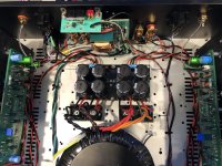
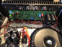
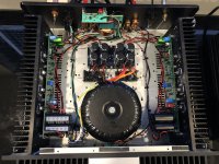
I just finished my AB100 in an old Rotel case, with boards from Alexcp.
Rails at +/-51V and 27000Uf capacitance per rail. I am worried about those caps are rated 50V. Offset 10mV one channel and about 20mV the other one.
The heatsinks are full of holes because I built 3 amps in that case, F5, F6, and F7, and now AB100
With bias at 20ma per transistor and Re 1 ohms the heatsinks are cold.
I want to improve this amp by changing the emitter resistors and adjust the bias for lowest possible distortion. D. Self mentioned to use 0.1 ohms resistors. Did anyone use 0.1R emitter resistors?
Attachments
Looks cool!
I have not tried 0.1ohm with the AB100, but there should be no problem, you would only need to adjust the bias again.
I have not tried 0.1ohm with the AB100, but there should be no problem, you would only need to adjust the bias again.
The lower the resistance, the more any mismatching shows up, so as you
adjust the overall bias, you need to check current through individual transistors,
and watch over them as they warm up.
adjust the overall bias, you need to check current through individual transistors,
and watch over them as they warm up.
So, matched outputs would allow the use of lower (or none?) emitter resistors, with less NF...
How does class AB sound/perform under (near) matched output devices?
How does class AB sound/perform under (near) matched output devices?
Just sharing my thoughts - it is hard to keep output devices matched because their properties changes over temperature. For low signal transistors, this is okay since their changes are very minimal over temperature and with respect to the signal levels or voltages they are operating at.
Running parallel outputs without degeneration resistor can also cause imbalance power loading, leading to a device or some of the devices having most of the power, while some have less. This leads to early design failures.
The only configuration I would consider no degeneration resistor are those with a single pair output, and the output devices are rated multiple times the maximum amplifier rating (including the power supply). For example, you are designing an amplifier capable of 40W-50W, while using output devices rated for 300W or higher. You also need to make sure the thermal stability of the amp, as well as limit your power supply output in case of overload conditions.
The transistors are not matched. The degeneration resistors are 1%.
It seems that is too dangerous to use 0.1R resistors so I will try 0.5R and adjust the bias to 50mA per transistor.
It seems that is too dangerous to use 0.1R resistors so I will try 0.5R and adjust the bias to 50mA per transistor.
Why do you assume the degeneration resistors are perfectly matched over temperature?
Hi Mark, of course, those resistors change over temperature. But their error is insignificant compared to the stability they add to the circuit.
Even if the resistors have huge tolerance (including drifts due to temperature), just having "any" degeneration resistance improves the linearity of the output base on the Vbe voltage.
It is hard to explain over text, I would have to create a video to explain the nodal analysis. I did a quick search and I found this link could help explain the behavior: https://www.electronics-tutorials.ws/amplifier/emitter-resistance.html
As I mentioned before, the resistor values dictate the balancing of the load current when you are considering a bank of devices.
However, power resistors tend to have the same temperature coefficient --- meaning, the resulting drifts on all the resistors will be on the same direction and will most likely be close to each other. This effect will maintain an even load balancing across the devices.
According to my spice simulator results for AB100 -
reducing Re and increasing the bias - slightly (from 0.006 to 0,004 decreases THD at a small power (1W), but at 20W the reduction is negligible.
as mentioned above - measure the voltage drop across each individual resistor - if they are the same (in range few mV) - you can further reduce Re, the question is whether it makes sense- either just by increasing the class A region and heat.
I measured with sound card my AB 100 amps - first one with just one pair MJ11016 / 15 + -37V 100mA per transistor Re 0.235R) and for the second with 2 pairs MJ11016 / 15 + -43V 50mA per transistor Re 0.5R):
I measured around 0.006 and 0.008% THD at 8 R load and 3V RMS (1W approx). But I think that the VA transistor had a bigger impact here, because in the second variant I have MJ340 and MJ350, which are not the best choice, this is also confirmed by LT spice.
Hello Osscar, what you said is absolutely true. Thanks for answering the 2nd part of the question -- regarding sound.
What I was really answering was regarding "matched outputs" and the "possibility of removing Re". Please see post #1049.
My answers are:
1. Matching the outputs is not important! Because the output devices generate heat, having them perfectly matched at certain temperature does not guaranteed they are still matched after 5 mins of use.
2. In a DIY context, never remove Re - this is a big NO NO! You run the risk of serious thermal issues due to output loading.
The follow-up question was regarding the "matched resistors with respect to temperature", and my answers was:
1. Resistor matching is not required - as long as there is an Re. Your statement also supported this.
2. Additionally --- unlike thin film resistors where the thermal coefficient could be (+) or (-) depending on how they trim the parts, power resistors have tend to have the same thermal coefficient. So for an output bank, this means the tolerance will vary in the same direction, and will mostly like have the same tolerance effects. So in other words, it doesn't matter.
Finally, adding to your statement regarding reducing Re value --- as Nelson said it - as you lower the Re, the more the effects of the imbalance will show up. Sound-wise, yes there is improvement as shown in your PSPICE simulation, but you run the risk of thermal issues.
So it is a balancing act - you improve the performance and sound by a little bit (negligible per your simulation), but also risks load imbalance and thermal issue on the other hand.
This question is for Nelson. Is it possible to change the front end to accept balanced signal?
Gain Question
Hi Guys,
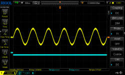
Finally managed to put my boards together, and mounted on a heatsink for some intial testing, and I noticed something weird.
I was feeding the amp a 1kHz sine wave at about .1V and was getting about 20V at the output on the scope.
That would seem to me the gain is somewhere at 200 and I though it was supposed to be in the order of 20.
I have about 2.5-3 amps as per rail current going but nothing changes even if I turn down the resistor all the way so the current is like .1 amps, still getting about 20V output.
Any thoughts, since its an order of 10 off I was thinking maybe somewhere I have a part wrong, but short of checking them all anybody have any ideas?
What parts exactly control the gain factor?
Will post some pics of the scope traces and the board later.
Thanks all
Hi Guys,
Finally managed to put my boards together, and mounted on a heatsink for some intial testing, and I noticed something weird.
I was feeding the amp a 1kHz sine wave at about .1V and was getting about 20V at the output on the scope.
That would seem to me the gain is somewhere at 200 and I though it was supposed to be in the order of 20.
I have about 2.5-3 amps as per rail current going but nothing changes even if I turn down the resistor all the way so the current is like .1 amps, still getting about 20V output.
Any thoughts, since its an order of 10 off I was thinking maybe somewhere I have a part wrong, but short of checking them all anybody have any ideas?
What parts exactly control the gain factor?
Will post some pics of the scope traces and the board later.
Thanks all
If we refee to the circuit in the first post ... r3 and r4 determine the gain....but it sounds strange...
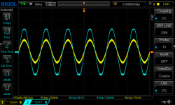
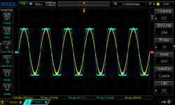
Hi All,
So much thanks for the quick replies,
so it looks like R3 & R4 are correct, I did notice that R14 is only 3.5k instead of 6.8k, think this could be the problem?
Also here are the scope traces
So much thanks for the quick replies,
so it looks like R3 & R4 are correct, I did notice that R14 is only 3.5k instead of 6.8k, think this could be the problem?
Also here are the scope traces
Attachments
- Home
- Amplifiers
- Pass Labs
- AB100 Class AB Power Amplifier