You may try with 4700uF as it is local decoupling, ... Have a beefy PSU.
The sponsored layout with TO-3 that I did for a customer , has provision for 35mm dia caps.
Regards
Prasi
The sponsored layout with TO-3 that I did for a customer , has provision for 35mm dia caps.
Regards
Prasi
Last edited:
This would be a long read post.  Sorry for that.
I may consider in future to order quality PCB's from gerbers, something I never did before.
And there was something I knew I want: 2mm PCB thickness, 2oz copper thickness, interesting or base green solder mask color and ENIG surface finish.
I went on JLCPCB and PCB Way page for comparison and saw there is "Thickness of Immersion Gold" for ENIG on PCB Way page.
Choices are 1U", 2U", 3U" and no thickness choice for ENIG on JLCPCB page.
Next days there was a seach for more information what does it mean.
My guess is U" stands for micro inches and most probably for gold thickness.
There is a specification for ENIG called PC-4552 (IPC Standard).
Electroless Nickel Thickness: 3 to 6 µm [118.1 to 236.2 µin]
ENIG - Soldering Applications Only: The minimum immersion gold deposit thickness shall be 0.04 µm [1.58 µin] at -4 sigma from the mean as measured on a pad size of 1.5 mm x 1.5 mm [0.060 in x 0.060 in] or equivalent area.
No max range for Au thickness on PC-4552 specification.
More google seach for info and:
The typical gold thickness range is 0.075 µm to 0.125 µm [2.95 µin to 4.92 µin].
Gold thickness above 4.925 µ" can indicate increased risk of having compromised the integrity of the nickel undercoat due to excessive corrosion.
More search and I found there is a more fresh and strict revision ENIG specification IPC4552 Revision A (IPC-4552A):
Au: 0.04-0.1um (1.58-3.94uin) with a +/- 3 sigma standard deviation applied
Ni: 3-6um (118.1-236.2uin)
There is a good read about ENIG here:
ACHIEVING A SUCCESSFUL ENIG FINISHED PCB UNDER REVISION A OF IPC 4552 MACDERMID ENTHONE
https://electronics.macdermidenthon...sion_A_of_IPC_4552_Bunce_Martin_SMTA_2017.pdf
A bit from this read:
The first order of change is the gold deposit thickness control and measurement.
The specification draws attention to the accuracy of the equipment currently in the field. Significant advancements have been made in X-ray fluorescence measurement equipment but that technology costs on the order of $100k which not all PCB fabricators can justify owning.
For the gold layer, there has been a reduction of the minimum allowable thickness and a new maximum thickness set.
Extremely low gold thickness contributes to performance failures as a thin deposit may not last through thermal conditioning and environmental exposure, remembering this was two of the desired advantages offered by the ENIG finish.
The upper limits help to combat the potential nickel corrosion caused with excessive galvanic displacement required to drive the deposition mechanism.
Today’s specification contains a section dedicated to measuring the phosphorous content of the electroless nickel deposit.
The 4552 revision introduces a new measurement system for phosphorous content and process control requirements that the PCB fabricator is required to demonstrate.
Lastly, there is a clear explanation for evaluating an ENIG deposit for corrosion. It contains a suggested evaluation method and levels of acceptability.
Gold is deposited onto a nickel surface through an exchange reaction also called an immersion or galvanic displacement reaction.
To deposit gold onto the electroless nickel surfaces, electrons must be transferred from the metallic electroless nickel deposit to the gold ions in solution producing a metallic gold deposit.
This electron transfer results in removal of metallic nickel (corrosion) from the surface of the electroless nickel deposit and builds up nickel ions in the immersion gold solution as the reaction proceeds.
Traditional immersion gold systems can allow uncontrolled dissolution of nickel metal and result in localized undesired spikes of corrosion which can be viewed in top down microscopy or through cross section.
Due to the nature of the gold plating mechanism, there will always be some level of corrosion as nickel must be removed from the electroless nickel deposit surface to facilitate the gold metal deposition.
It is the level as seen both in amount over the surface and depth of that corrosion that is the concern.
Excessive corrosion can result in poor IMC formation and weaker solder joint formation which in turn can cause components to fall from the Printed Circuit Board Assembly (PCBA) surface.
...
A few conclusions.
Gold in ENIG is is only to ptotect nickel from oxidizing.
Gold a waste product that will be absorbed into the solder joint.
Gold thickness results below the specified range may result in insufficient oxidation resistance for the nickel.
Gold thickness results above the specified range may result in an attack on the nickel itself. The nickel may corrode and ultimately result in black pad if aggressive enough. The thicker the gold, the greater the risk for black pad.
So.. back to PCB Way ENIG thickness.
If 1U" stands for 1 micro inches then it is lower than any PC-4552 standard specification.
Or am I wrong?
Sorry for that.I may consider in future to order quality PCB's from gerbers, something I never did before.
And there was something I knew I want: 2mm PCB thickness, 2oz copper thickness, interesting or base green solder mask color and ENIG surface finish.
I went on JLCPCB and PCB Way page for comparison and saw there is "Thickness of Immersion Gold" for ENIG on PCB Way page.
Choices are 1U", 2U", 3U" and no thickness choice for ENIG on JLCPCB page.
Next days there was a seach for more information what does it mean.
My guess is U" stands for micro inches and most probably for gold thickness.
There is a specification for ENIG called PC-4552 (IPC Standard).
Electroless Nickel Thickness: 3 to 6 µm [118.1 to 236.2 µin]
ENIG - Soldering Applications Only: The minimum immersion gold deposit thickness shall be 0.04 µm [1.58 µin] at -4 sigma from the mean as measured on a pad size of 1.5 mm x 1.5 mm [0.060 in x 0.060 in] or equivalent area.
No max range for Au thickness on PC-4552 specification.
More google seach for info and:
The typical gold thickness range is 0.075 µm to 0.125 µm [2.95 µin to 4.92 µin].
Gold thickness above 4.925 µ" can indicate increased risk of having compromised the integrity of the nickel undercoat due to excessive corrosion.
More search and I found there is a more fresh and strict revision ENIG specification IPC4552 Revision A (IPC-4552A):
Au: 0.04-0.1um (1.58-3.94uin) with a +/- 3 sigma standard deviation applied
Ni: 3-6um (118.1-236.2uin)
There is a good read about ENIG here:
ACHIEVING A SUCCESSFUL ENIG FINISHED PCB UNDER REVISION A OF IPC 4552 MACDERMID ENTHONE
https://electronics.macdermidenthon...sion_A_of_IPC_4552_Bunce_Martin_SMTA_2017.pdf
A bit from this read:
The first order of change is the gold deposit thickness control and measurement.
The specification draws attention to the accuracy of the equipment currently in the field. Significant advancements have been made in X-ray fluorescence measurement equipment but that technology costs on the order of $100k which not all PCB fabricators can justify owning.
For the gold layer, there has been a reduction of the minimum allowable thickness and a new maximum thickness set.
Extremely low gold thickness contributes to performance failures as a thin deposit may not last through thermal conditioning and environmental exposure, remembering this was two of the desired advantages offered by the ENIG finish.
The upper limits help to combat the potential nickel corrosion caused with excessive galvanic displacement required to drive the deposition mechanism.
Today’s specification contains a section dedicated to measuring the phosphorous content of the electroless nickel deposit.
The 4552 revision introduces a new measurement system for phosphorous content and process control requirements that the PCB fabricator is required to demonstrate.
Lastly, there is a clear explanation for evaluating an ENIG deposit for corrosion. It contains a suggested evaluation method and levels of acceptability.
Gold is deposited onto a nickel surface through an exchange reaction also called an immersion or galvanic displacement reaction.
To deposit gold onto the electroless nickel surfaces, electrons must be transferred from the metallic electroless nickel deposit to the gold ions in solution producing a metallic gold deposit.
This electron transfer results in removal of metallic nickel (corrosion) from the surface of the electroless nickel deposit and builds up nickel ions in the immersion gold solution as the reaction proceeds.
Traditional immersion gold systems can allow uncontrolled dissolution of nickel metal and result in localized undesired spikes of corrosion which can be viewed in top down microscopy or through cross section.
Due to the nature of the gold plating mechanism, there will always be some level of corrosion as nickel must be removed from the electroless nickel deposit surface to facilitate the gold metal deposition.
It is the level as seen both in amount over the surface and depth of that corrosion that is the concern.
Excessive corrosion can result in poor IMC formation and weaker solder joint formation which in turn can cause components to fall from the Printed Circuit Board Assembly (PCBA) surface.
...
A few conclusions.
Gold in ENIG is is only to ptotect nickel from oxidizing.
Gold a waste product that will be absorbed into the solder joint.
Gold thickness results below the specified range may result in insufficient oxidation resistance for the nickel.
Gold thickness results above the specified range may result in an attack on the nickel itself. The nickel may corrode and ultimately result in black pad if aggressive enough. The thicker the gold, the greater the risk for black pad.
So.. back to PCB Way ENIG thickness.
If 1U" stands for 1 micro inches then it is lower than any PC-4552 standard specification.
Or am I wrong?
Last edited:
Gold looks nice though, doesn't it?
😉
It does.
PCB's looks very pretty. 😀
Gold looks nice though, doesn't it?
😉
Nice one!😉
I have seen clear (transparent) solder mask on gold flash PCB
Nice one!😉
I have seen clear (transparent) solder mask on gold flash PCB
Oh yeah, Gold Flash A.K.A: Flash Gold, Hard Gold, Electrolytic Gold, Full body Hard Gold, Tab Gold, Selective Gold.
I made a few searches about it too. 🙂
The maximum thickness that IPC considers to be solderable is 17.8 µin
And PCB Way can offer Hard Gold with minimum thickness Au:3U"/Ni120U"
I wonder would't it would be too hard to solder. 🙄
So I decided it would be 2.0mm thick FR4 (TG 13-140) boards.
Purple solder mask.
ENIG (2U") finish.
2oz copper.
With (Not to add extra pcb product number on board) option.
Kind of expensive because of extra $ color and 2U" ENIG finish.
Are there any interest to cut the cost with quantity?
P.S.: Not asking for money just gather interest.
Precalculated price on PCB Way page for 20 pcs (10 pairs) is $205 minus $10 discount coupon = $195
Shipping to my house:
1. $28 e-packet (15-30 days)
2. $45 EMS (10-15 days)
3. $59 DHL (3-5 days)
Purple mask with ENIG looks awesome.
Although you will not see any gold after solder.. 😀
But it is definately rare color for DIY Pass boards.
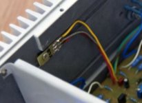
As far as build goes does the ZTX 450 at Q8 make contact with the heatsink for thermal tracking? And if so how did people achieve that? Mounting to the underside?
Does a jumper need to go into the C9 position if no cap is used
No, nothing needed.
Does a jumper need to go into the C9 position if no cap is used
Does the Q8 transistor make contact with heatsink. How do people acheive that?
Maybe on original PCB Q8 can be soldered on the other side of PCB at the correct height so that it touches the heat-sink ?
In my boards i use a small diy pcb which i screw on the heatsink (Please find attached pics - this principle can be applied to small bias transistors) .I've also seen factory made transistor holders, but they are rare.
In my boards i use a small diy pcb which i screw on the heatsink (Please find attached pics - this principle can be applied to small bias transistors) .I've also seen factory made transistor holders, but they are rare.
Attachments
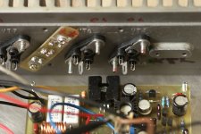
So I notice you are extending yours with leads. Does that present any issues? I could extend mine from leads that are a 2-3 inch long. Can that cause any instability issues? The schematic calls out a ZTX450 for Q8. What are you using? It would be nice if I could use something that would have a screw down package like TO220 or something.
No problems with extended leads/wires. In first ab100 i used ztx450, in second one i used BD 139...here is nice diy solution for mounting bracket:
An easy way to mount DS18B20 temperature sensors | Matt's Tech Pages
An easy way to mount DS18B20 temperature sensors | Matt's Tech Pages
Excellent ossar. I love this forum. BTW are the to open holes on the NP pcb toward the front for the signal hot and ground?
Also question on biasing. What value pot did you end up using? what current level through each transistor did you settle on? I'm using .68ohm emitter resistors volts drop/.68 will be the current correct?
i used 4k7 or 5K multi turn pot.
Regarding bias - my standard setup are 100mA per transistor with 0.22RE and about 50-60mA per transistor with 0,5RE. In AB100 article total bias current 80mA indicated - so it 20mA per transistor ( 4 on each rail) .
regarding bias measurement - yes across 0,68R 50mA = 34mV. ( 50mA may be to much if four pairs used = total bias current will be 200mA ) 20mA approx 14mV. When you start to adjust bias - pot should be set to max. resistance. Lower resistance = higher bias.according to D.Self higher RE value=lower bias optimum value.
sorry i didn't study NP board signal ground connection...i can take a look later.
Last edited:
Just wanted to weigh in. Biasing up mine now. Everything going great! Outside in shop where it is 98 Deg F. No problems very stable on a big heatsink.
BTW just wondering why so many people are fretting over Darlington output stage. I have been living with an A40 for 10 years. It is simple and a beautiful sounding amp. If this is similar in design I have high hopes on it's sound. Must say I lived with the Adcom 555 for 10 years also and loved it.
Will keep people posted.
- Home
- Amplifiers
- Pass Labs
- AB100 Class AB Power Amplifier