Hi,
@Christian
in #64 You asked about increasing driver current.
That won´t help. While with the EF the output transistors basically supply for all the load and idle current alone, all the CFP transistors combine their currents.
So when the output transistor cuts off the driver transistor´s current is deformed from the sinusodial shape and THD of the higher harmonics shoots up.
Raising its idle current only raises the level where the deformation occurs and/or the driver cuts off also.
With the EF one only needs to ensure that the driver runs hot enough that it supplies for the output transistors base current.
jauu
Calvin
Change the values for the resistors in the collector and emitter connections of Q3 and Q5 to 100R. I have to go out - I will given my reasoning for this later.
Change the values for the resistors in the collector and emitter connections of Q3 and Q5 to 100R. I have to go out - I will given my reasoning for this later.
Looking at Q5 and Q6 "Darlington-in" NPN half section.
The current flow in these transistors is from emitter to collector with perhaps 1% passing through the base in both cases. The effect of the base current of Q6 on the emitter current of Q5 is negligible.
R5 needs to be capable of passing sufficient current to drop sufficient enough of a d.c. voltage to establish adequate boundaries for impressed a.c. signals to ride on. Too high a resistor value for R5 will be limiting factor - I see that as the likely cause of the problem.
I suggested the same values for R4 and R5 to balance on either side of Q5.
Just a quick reply esp to mjona and other klever kiwis. I have got a lot to say on the back of today's investigation but there are one or two things I want to try before giving a proper report.
The hints are that the 100R + 100R doesn't work - and I have reasons for that, having looked at the switch off (and I think Douglas may be wrong here because he too uses 100R in the R4 position in his Trimodal amp - but I'll look further before I am so impertinent as to take that leap). One that point the currents are exactly what you'd expect in resistors that have been paralleled by a diode drop - so in both driver stages the current does seem to be being pulled or pushed through, if not especially firmly but the output transistor behaviour is much better and stays off for longer and switches on more quickly with more current through the bigger driver.
Another point is that the earlier change in distortion levels was down to going from Class A entirely to a badly set up Class AB (or B - I never know which to call it; the one where you aim to smooth out the gain in transition). Lower Iq of 50mA (through the output transistors, because about the same can be going through the drivers at the same time) works better, and I am going to work down from there - or do some head and wings graphs. Where I am at the moment is slightly odd because although the 2nd harmonic is 82dB down at 10V, there seems to be not much difference in the other harmonics.
I have changed the model and someone might like to point out its flaws, but it was quick and easy. The bandwidth has gone way back up (to 94MHz) but I also fear there's a flaw in the BD139/140 models. I don't know the parameter or how it works (XTF) but the value seems odd. I have got some other BD models and may standardise on the LT_Wiki standard.bjt.
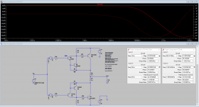
I can post the circuit and the crossover behaviour as it is currently (and on that if you lower the driver current the period of flatness more than halves, rounding off at the sides.). The driver current also looks that much less nimble. Incidentally the driver current is actually positive, though this way up separates them out better. So driver + output current does equal Re current.
Ah, have to go advanced for the piccies.
The hints are that the 100R + 100R doesn't work - and I have reasons for that, having looked at the switch off (and I think Douglas may be wrong here because he too uses 100R in the R4 position in his Trimodal amp - but I'll look further before I am so impertinent as to take that leap). One that point the currents are exactly what you'd expect in resistors that have been paralleled by a diode drop - so in both driver stages the current does seem to be being pulled or pushed through, if not especially firmly but the output transistor behaviour is much better and stays off for longer and switches on more quickly with more current through the bigger driver.
Another point is that the earlier change in distortion levels was down to going from Class A entirely to a badly set up Class AB (or B - I never know which to call it; the one where you aim to smooth out the gain in transition). Lower Iq of 50mA (through the output transistors, because about the same can be going through the drivers at the same time) works better, and I am going to work down from there - or do some head and wings graphs. Where I am at the moment is slightly odd because although the 2nd harmonic is 82dB down at 10V, there seems to be not much difference in the other harmonics.
I have changed the model and someone might like to point out its flaws, but it was quick and easy. The bandwidth has gone way back up (to 94MHz) but I also fear there's a flaw in the BD139/140 models. I don't know the parameter or how it works (XTF) but the value seems odd. I have got some other BD models and may standardise on the LT_Wiki standard.bjt.
I can post the circuit and the crossover behaviour as it is currently (and on that if you lower the driver current the period of flatness more than halves, rounding off at the sides.). The driver current also looks that much less nimble. Incidentally the driver current is actually positive, though this way up separates them out better. So driver + output current does equal Re current.
Ah, have to go advanced for the piccies.
Pictures and asc as interim.
Sorry, forgot to press Upload.
Attachments
Just a quick reply esp to mjona and other klever kiwis. I have got a lot to say on the back of today's investigation but there are one or two things I want to try before giving a proper report.
There are two "Aussies" and one "Kiwi" on board this thread.
Sorry, forgot to press Upload.
A general question: Why do you use a triple output stage with such small power levels? Do you have special VAS requirements?
I would like to see a modern output stage which does something against the typical problems: beta droop at higher current, gm-doubling, early effect, SOAR limitations at higher voltages, non-linear C_CB capacitance in the driver and bias current temperature dependency.
AC analysis is problematic as there is no well defined operating point in an output stage. The results depend strongly at the VAS source impedance which are often not realistic.
Hi!I would like to see a modern output stage which does something against the typical problems: beta droop at higher current, gm-doubling, early effect, SOAR limitations at higher voltages, non-linear C_CB capacitance in the driver and bias current temperature dependency.
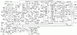
Here is a diagram of the amplifier, where it is all taken into account and taken measures to avoid these effects. This amplifier was built 1999 year our specialist on measurements in nuclear physics.
The first stage of the follower has 2 transistors on the shoulder - VT16, VT18. The second stage (the driver) has 4 transistors in the shoulder: VT20 - VT23. The output stage follower contains 8 transistors.
Attachments
Last edited:
The hints are that the 100R + 100R doesn't work - and I have reasons for that, having looked at the switch off (and I think Douglas may be wrong here because he too uses 100R in the R4 position in his Trimodal amp - but I'll look further before I am so impertinent as to take that leap). One that point the currents are exactly what you'd expect in resistors that have been paralleled by a diode drop - so in both driver stages the current does seem to be being pulled or pushed through, if not especially firmly but the output transistor behaviour is much better and stays off for longer and switches on more quickly with more current through the bigger driver.
Another point is that the earlier change in distortion levels was down to going from Class A entirely to a badly set up Class AB (or B - I never know which to call it; the one where you aim to smooth out the gain in transition). Lower Iq of 50mA (through the output transistors, because about the same can be going through the drivers at the same time) works better, and I am going to work down from there - or do some head and wings graphs. Where I am at the moment is slightly odd because although the 2nd harmonic is 82dB down at 10V, there seems to be not much difference in the other harmonics.
I have changed the model and someone might like to point out its flaws, but it was quick and easy. The bandwidth has gone way back up (to 94MHz) but I also fear there's a flaw in the BD139/140 models. I don't know the parameter or how it works (XTF) but the value seems odd. I have got some other BD models and may standardise on the LT_Wiki standard.bjt.
You will have to get other advice about the sim files for BD139/140 that is not my thing, however the bandwidth of the complete amplifier will be limited by that of the output devices and changes in phase due to time delays caused by stored charges in the base regions of the output devices. These persist after the signal voltage has been removed.
As a general rule the frequency response of the voltage amplification stage has to be rolled off well below the frequencies you have been looking at. Pushing the bandwidth of the drivers I see as barking up the wrong tree.
You should be looking at current available from Q6 to charge/discharge the base of the power transistor - Cordell gives a formula to calculate that requirement - there is an article on his website entitled "Another View of TIM" giving the details.
When you have sorted out this detail then you can see what value resistance you might need for R4.
... like to point out its flaws, but it was quick and easy. The bandwidth has gone way back up (to 94MHz) but I also fear there's a flaw in the BD139/140 models. I don't know the parameter or how it works (XTF) but the value seems odd...
I don't understand, why have you altered the model? Based on what data?
XTF affects the drop-off of ft at hi currents so if you twiddle it you can certainly improve the bandwidth of the simulation, but that won't help reality of course.
What is the new model and what looks odd?
Best wishes
David
I don't understand, why have you altered the model? Based on what data?
XTF affects the drop-off of ft at hi currents so if you twiddle it you can certainly improve the bandwidth of the simulation, but that won't help reality of course.
What is the new model and what looks odd?
Best wishes
David
I didn't alter the model. It's downloaded from Bob Cordell's site. XTF is set at 10,000. And where it is mentioned elsewhere, if at all, it is in single figures. That's one of the things for today, to work out why it seems so transistor sensitive. Here is the text of the models.
* BD139C - created April 13, 2011 copyright Cordell Audio
.MODEL BD139C npn
+IS=150e-15 BF=260 VAF=99
+IKF=1.2 ISE=70e-15 NE=1.2 NF=1.0
+RB=5 RC=0.01 RE=0.08
+CJE=293e-12 MJE=0.33 VJE=0.67
+CJC=49e-12 MJC=0.39 VJC=0.52 FC=0.5
+TF=585e-12 XTF=10000 VTF=35 ITF=20
+TR=10e-9 BR=78 IKR=0.14
+EG=1.21 XTB=1.14 XTI=3 NC=1.45
+ISC=19e-12 NR=1.0 VAR=7.5 IRB=0.03
+RBM=0.001 XCJC=0.53 mfg=CA041311
*
*
* BD140C - created April 13, 2011 copyright Cordell Audio
.MODEL BD140C pnp
+IS=120e-15 BF=113 VAF=140
+IKF=1.5 ISE=1000e-15 NE=1.5 NF=1
+RB=5 RC=0.01 RE=0.1
+CJE=220e-12 MJE=0.35 VJE=0.7
+CJC=68e-12 MJC=0.35 VJC=0.6 XCJC=0.5 FC=0.5
+TF=320e-12 XTF=10000 VTF=35 ITF=20
+TR=100e-9 BR=25 IKR=0.1
+EG=1.2 XTB=1.5 XTI=3 NC=1.4
+ISC=7e-12 NR=1.0 VAR=8 IRB=0.01 RBM=0.01 mfg=CA041311
There are two "Aussies" and one "Kiwi" on board this thread.
Sorry about this mistake. Geography was never a strong subject.
I don't understand, why have you altered the model?
I see what you were getting at. I had changed the circuit to get a low impedance source and to get rid of the 47k resistors and that possible path. It was just a quick thing so I could get a proper look at the input (which is just about on 0dB, bar some capacitance) and keep the output stage in isolation. You can see it on page 9.
You will have to get other advice about the sim files for BD139/140 that is not my thing, however the bandwidth of the complete amplifier will be limited by that of the output devices and changes in phase due to time delays caused by stored charges in the base regions of the output devices. These persist after the signal voltage has been removed.
As a general rule the frequency response of the voltage amplification stage has to be rolled off well below the frequencies you have been looking at. Pushing the bandwidth of the drivers I see as barking up the wrong tree.
You should be looking at current available from Q6 to charge/discharge the base of the power transistor - Cordell gives a formula to calculate that requirement - there is an article on his website entitled "Another View of TIM" giving the details.
Rather than be dominated by the output transistor, as in a standard EF, the CFP ends up giving the geometric mean of the fts and what seems to be happening from looking at the phase response is that we aren't getting 3 separate poles - and it seems even that some of the capacitance is coming into play to our advantage. What I am trying to do here is to make sure that the parameters don't combine destructively, leaving us with peaks in the MHz region. The actual bandwidth itself will be much less and will be properly defined, probably as a third order Butterworth around 150kHz with two poles on the output of the pre-amp and the third on the input of the power. I'm not that averse to putting a small cap across the drivers for this in the end as I'm told that the bottom half of CFPs almost always oscillate. But I am keen that this doesn't show up inductively at the output. Things yet to be done include looking at changes in impedance under load etc.
I'm always happy to read what Bob Cordell has to say so will go there right away. I assume you mean Q4.
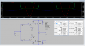
If I get the chance later today I'll show you what the switch off looks like when you starve Q4 of current, ie with 47R or 100R Essentially the flat part of Ic falls to less than half the duration and becomes much more sinusoidal. You can do this yourself with the asc posted, it's just a bit of a fiddle setting the Iq, which I am now running at 50mA and planning to go lower.
A general question: Why do you use a triple output stage with such small power levels? Do you have special VAS requirements?
The results depend strongly at the VAS source impedance which are often not realistic.
The voltage is arbitrary at the moment. I think I would always use a triple because it presents a very much higher impedance to the VAS and so won't modulate the load that the VAS sees. When the loudspeaker impedance multiplied through output stage it will vary the amount of gain available at different frequencies. I think this is one of the key reasons people seem to like small amounts of feedback and it has nothing to do with the feedback itself. If you have a small load at the top of the VAS (and much less gain and and therefore less feedback) then it will dominate the load in parallel with it, being the multiplied version of the loudspeaker impedance. Increase the notional load to effectively infinity, as with an active load, and the only load the VAS sees is the loudspeaker, complete with its reactive components. I have had this idea for some time and then saw that John Curl uses a fet to present a high impedance to the VAS and get round this problem.
Rather than be dominated by the output transistor, as in a standard EF, the CFP ends up giving the geometric mean of the fts and what seems to be happening from looking at the phase response is that we aren't getting 3 separate poles - and it seems even that some of the capacitance is coming into play to our advantage. What I am trying to do here is to make sure that the parameters don't combine destructively, leaving us with peaks in the MHz region. The actual bandwidth itself will be much less and will be properly defined, probably as a third order Butterworth around 150kHz with two poles on the output of the pre-amp and the third on the input of the power. I'm not that averse to putting a small cap across the drivers for this in the end as I'm told that the bottom half of CFPs almost always oscillate. But I am keen that this doesn't show up inductively at the output. Things yet to be done include looking at changes in impedance under load etc.
I'm always happy to read what Bob Cordell has to say so will go there right away. I assume you mean Q4.
If I get the chance later today I'll show you what the switch off looks like when you starve Q4 of current, ie with 47R or 100R Essentially the flat part of Ic falls to less than half the duration and becomes much more sinusoidal. You can do this yourself with the asc posted, it's just a bit of a fiddle setting the Iq, which I am now running at 50mA and planning to go lower.
I have a problem with the SPICE I downloaded - I have been meaning to get my IT worker brother to look at this.
The stored charge issue relates to Q6 - PNP transistors present a little more difficulty than NPN - you can look up this point on the net.
Re changing the emitter resistors to 0.1 ohms and reducing the standing current below 50 m.a. - I see that as a move in the wrong direction.
Re bandwidth limiting - the inverting input where the feedback connects provides a path for signals to re-enter the amplification process. A speaker is a electro-motor.
If the closed loop of the amplifier has a gain of one at any frequency that is positive in phase it will oscillate even with no signal input or load connected.
The phase changes from positive to negative at 180 degrees but some safety margin is needed to guarantee stability. A rule of thumb is to reduce the gain to less than one at a frequency of 135 degrees.
The only effective way to achieve this is to by "compensating" the main voltage amplification stage.
Greater closed loop bandwidth comes at the cost of some compromise with stability.
If you push the closed loop bandwidth there will be an increasing risk of instability beyond 100 kHZ. This is due to the relative sluggishness of power transistors.
As long as your driver stage behaves within the chosen closed loop bandwidth that is all you should need to worry about.
An input filter stops what goes in the front door - but has no control over back door entry.
I have a problem with the SPICE I downloaded
Re changing the emitter resistors to 0.1 ohms and reducing the standing current below 50 m.a. - I see that as a move in the wrong direction.
You can download a new copy of LTspice at Linear.com. The standard.bjt that I am using can be found here. Standard.bjt - LTwiki-Wiki for LTspice . It has the Cordell models in it but is missing some of the Zetex models that I had before. Those can be found at Diodes Inc.
A speaker is a electro-motor.
This is a totally overstated point that appears to make sense to people who have heard the words "back EMF". They probably imagine that the amplifier has a rigid grip over the motion of the cone too. Even at a damping factor of infinity it doesn't. It might let stuff through outside its bandwidth and that's why you have your pole extending resistors, zobel networks etc., but that has nothing to do with the movement of the speaker cones. The important concept here is that it is an essentially an AC ground.
If the closed loop of the amplifier has a gain of one at any frequency that is positive in phase it will oscillate even with no signal input or load connected. The phase changes from positive to negative at 180 degrees but some safety margin is needed to guarantee stability. A rule of thumb is to reduce the gain to less than one at a frequency of 135 degrees.
Yes, I am aware of the basics of feedback. Have you looked at how little phase shift this circuit is managing - albeit in simulation? What appears to be happening is that rather than showing up as inductive impedances at the output and being a cascade of 3 separate poles, they aren't even managing the shift of a single pole. I will get to the bottom of this, but what one doesn't have is that sharp phase shift at the beginning of rolloff. I suspect that there are capacitative routes to the too of the emitter resistors and these actually send the phase back towards zero.
The only effective way to achieve this is to by "compensating" the main voltage amplification stage.
I disagree. From work that I have done on regulators a Miller cap is death to actual regulation. The same holds true in an ordinary amplifier. There are all sorts of places that movement in the rails finds its way onto the signal, from the Early effect simply dropping it there 70dB down, to PN junctions which will do it 0.6V down. And, no, a current source does not stop a voltage change on the rails appearing in the signal. One needs to maintain the same loop gain right across the band of interest. Then, since you were talking about it, the signal fed to it should be at a level such that the loop gain available to it is maintained or bettered even while the amplifier is losing its OLG.
If you push the closed loop bandwidth there will be an increasing risk of instability beyond 100 kHZ. This is due to the relative sluggishness of power transistors.
Well these aren't 2MHz devices. They are at least a decade out beyond that. The hope of using a CFP in this or the sandwiched arrangement is that the geometric mean effect on the ft means that they will behave as a single device that outperforms the relatively sluggish power transistors.
All the best
Christian
... the circuit to get a low impedance source and to get rid of the 47k resistors and that possible path.
Ok, now I understand, you altered the circuit but you wrote "model" in the earlier post #83.
I am sorry that I didn't think to comment on source impedance earlier, because I also was initially mislead by this.
My case was the opposite of yours, I just had a V source for the tests, so zero impedance.
But it turned out some of the circuits were more sensitive to source impedance than others, even at low but realistic impedance.
As to the XTF parameter, it controls how fast the ft drops off at hi current.
More means a faster drop-off.
There is an issue here, that an unrealistic value may fit better over a limited domain, at the expense of worse fit elsewhere.
If your test data is in that limited domain then it looks OK.
So these implausible values worry me, there are similar issues with some other parameters where the issue is more obvious because the parameter has a physical interpretation, it's a resistance say, that just can't be correct.
Personally I wouldn't use an extreme value even if it fitted some points better.
There is an additional problem with XTF, my copy of Cordell's book has a cross-out on his equation 20.8 that explains XTF, so I must have believed it was mistaken.
But I can't remember what the mistake was, or how serious. Also, after the equation is "Procedure 8" and I suspect this has a typo, "TF" should be "ITF" I think.
So be careful, remember if you alter XTF it interacts with other parameters.
Best wishes
David
Last edited:
Ok, now I understand, you altered the circuit but you wrote "model" in the earlier post #83.
Yeah, I did. I don't do this all day every day so I can be a little less than precise. (In all fields, as it happens. 🙂 ) In fact I haven't looked at circuits as in depth as this in a couple of years.
I replaced the BD139/140 model with a model of the Fairchild version from the LTWiki standard.bjt. It seems to perform fine though I couldn't make it identical because that bjt file didn't have the ZTXs that I was using earlier. So I did an upgrade to FMMT624/723. They look a cracking pair of transistors. Bandwidth goes soaring out to 160MHz and everything still very well behaved. Of course one of the jobs will be to try and upset it again and the first stop will be the MJE243/253.
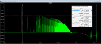
But so far, for the little work done today, it's looking promising. With a lower standing current of 15mA in the the main transistors and the 10R reinstated, we have the rather odd position of 50mA going through the drivers while 15mA goes through the output, but it's giving -100dB as the worst of all the distortion components. (There are a few of those and a few 10dB, or a third, below but it's still two zeros.) Since no one will believe me I enclose the FFT.
I'm out tomorrow evening and probably most of Saturday but I'll try and post up something everyone can work from as soon as I can. Sleep beckons now.
All the best
C
Attachments
Hi, ChristianThomas!
From experience, no the best output stage cannot have distortion less than 0.02...0.03% (20...30 ppm). You use in your models signal sources with zero output impedance. You're fooling yourself with this. Source of distortion is located at the entrance of the follower. By itself, your follower little distorts the signal, but distorted input currents into large output resistance of the VAS create a lot of distortion. Many amplifiers behave much better, than in practice, with signal sources with zero output impedance. Use more realistic conditions for the simulation.
I'm sorry for possible translation mistakes.
Attachments
- Status
- Not open for further replies.
- Home
- Amplifiers
- Solid State
- A three transistor compound pair?