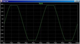
Anyone out there who has tried out the Blameless with two-pole compensation may have noticed that the amplifier then develops horrible, asymmetric squarewave, clipping and clipping recovery performance.
This is due to a number of issues - here the mods and additions I have made to address all of them.
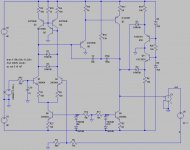
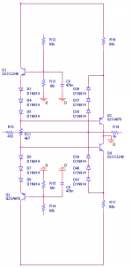
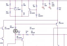
Firstly, a voltage clamp consisting of D3-D6 and transistors Q10 and Q11 is added which prevent saturation of the VAS transistor Q7 and its current source Q9. This comes at only a small cost to the output voltage swing.
Secondly, the LTP is provided with a 3-transistor current source and the VAS has an emitter degeneration resistance of 24 ohms. In this case the VAS standing current is 9mA and the LTP tail current is 5mA.
The result of this is that the quiescent, or DC voltage at the collector of each long tail pair transistor is equal.
This allows two back-to-back limiting diodes, D1 and D2, to clamp the maximum AC drive voltage to the VAS emitter follower symmetrically at +/-700mV.
This has two very important benefits. Firstly, it makes it impossible for the current mirror transistors to saturate. Secondly, the +/-700mV limited output swing automatically provides a current limit for the VAS, being equal to 700mV/24 ohms (R17), or ~30mA.
This is due to a number of issues - here the mods and additions I have made to address all of them.
Firstly, a voltage clamp consisting of D3-D6 and transistors Q10 and Q11 is added which prevent saturation of the VAS transistor Q7 and its current source Q9. This comes at only a small cost to the output voltage swing.
Secondly, the LTP is provided with a 3-transistor current source and the VAS has an emitter degeneration resistance of 24 ohms. In this case the VAS standing current is 9mA and the LTP tail current is 5mA.
The result of this is that the quiescent, or DC voltage at the collector of each long tail pair transistor is equal.
This allows two back-to-back limiting diodes, D1 and D2, to clamp the maximum AC drive voltage to the VAS emitter follower symmetrically at +/-700mV.
This has two very important benefits. Firstly, it makes it impossible for the current mirror transistors to saturate. Secondly, the +/-700mV limited output swing automatically provides a current limit for the VAS, being equal to 700mV/24 ohms (R17), or ~30mA.
Attachments
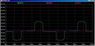
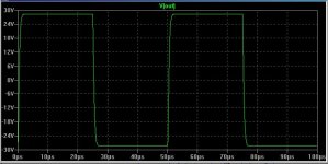
The next plot shows the collector voltages of the LTP transistors during clipping. The green trace is the collector voltage of Q1 and the pink trace is the collector voltage of Q2.
The red trace is the positive supply voltage. Note how D1 and D2 limit the voltage swing and how neither of the current mirror transistors can saturate.
The red trace is the positive supply voltage. Note how D1 and D2 limit the voltage swing and how neither of the current mirror transistors can saturate.
Attachments
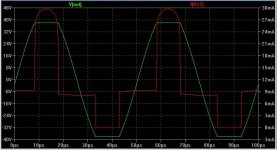
And finally here is a teaser pic of a complete design using this 2-pole input stage and VAS. Using a pair of optimally biased output transistors (class B) wrapped up in a CFB output stage it is rated at 100W into 4 ohms and simulates as follows at 20kHz, 50W into 8 ohms:
Harmonic Frequency Fourier Normalized Phase Normalized
Number [Hz] Component Component [degree] Phase [deg]
1 2.000e+04 2.828e+01 1.000e+00 -2.95° 0.00°
2 4.000e+04 1.939e-05 6.855e-07 179.75° 182.70°
3 6.000e+04 1.433e-05 5.065e-07 -150.49° -147.54°
4 8.000e+04 3.288e-06 1.163e-07 -10.90° -7.94°
5 1.000e+05 5.860e-06 2.072e-07 35.99° 38.94°
6 1.200e+05 4.653e-07 1.645e-08 -142.54° -139.58°
7 1.400e+05 3.085e-06 1.091e-07 -123.61° -120.65°
8 1.600e+05 1.149e-06 4.061e-08 -57.36° -54.40°
9 1.800e+05 2.595e-06 9.175e-08 -75.79° -72.84°
Total Harmonic Distortion: 0.000090%
The global unity loop gain frequency is 850kHz and the phase margin is 80 degrees.
I’m currently laying out the PCB for this one and will reveal the full circuit on my WWW when it’s up and running, along with a few other amps that are currently under construction.
This non-class-A one will be my cool running summer amp.
Attachments
G.Kleinschmidt said:
Secondly, the LTP is provided with a 3-transistor current source
current mirror?
Re: Re: A superior VAS clamp and VAS current limit for the Blameless.
Doh!
Yes, current mirror
It's after 11pm here.
pooge said:
current mirror?
Doh!
Yes, current mirror
It's after 11pm here.
Hi G. Kleinschmidt,
Are Q10 & Q11 and R19 & R16 really useful ?
I tested a somewhat similar configuration more than twenty years ago, inspired by the DB Systems DB6 amplifier.
I think that, keeping Q10 and Q11, the current through them could be used to used for a clipping indicator.
I don't remember exactly what was my circuit, I think part of the current through Q10 and Q11 returned to the inverting input.
looks like an adaptation of Cordell's front end protections to the Blameless
http://www.cordellaudio.com/papers/MOSFET_Power_Amp.pdf
you might want to point out the care needed to keep 0 V across the diff pair collector calmp D1,2 and that even with even mV bias the diodes have an impact on openloop gain with the hi-Z buffered input VAS (Pease "Trouble Shooting Analog Circuits")
perhaps the (reverse)biased diode bridge clamp I've shown in my composite op amp thread could reduce the impact of small Vos across the front end clamp:
http://www.diyaudio.com/forums/showthread.php?postid=512806#post512806
forr said:Hi G. Kleinschmidt,
Are Q10 & Q11 and R19 & R16 really useful ?
Most definately. 2-pole comp a very sensitive to any here the clipping isn't as clean if the clamp is removed.
Also, in a real circuit the VAS voltage clamp would be powered by the supply rails for the power output stage, preventing the VAS from being able to drive the driver (or pre-driver) transistors into saturation.
I also use this VAS clamp to indicate clipping in my designs. The collectors of Q10 and Q11 are just returned to ground via a resistor of a few hundred ohms. A window comparator is used to sense whenever the collector voltage deviates more than +/-100mV or so.
Cheers,
Glen
jcx said:you might want to point out the care needed to keep 0 V across the diff pair collector calmp D1,2 and that even with even mV bias the diodes have an impact on openloop gain with the hi-Z buffered input VAS (Pease "Trouble Shooting Analog Circuits")
Yikes! I don't think it is critical at all. The Miller comp cap is the dominant LTP load here.
I'm simulation you have to imbalance it so badly that the diodes actually start conducting to see any degradation in the amplifiers linearity.
Cheers,
Glen
AndrewT said:nice.
Would there be any advantage in using diode connected small signal transistors for D1 - D4?
I dont think so. That will just get you more capacitance. 1N4148 do a nice job but you could use some fancier Si diodes if you wanted to.
Cheers,
Glen
Have you seen this (Q6/Q21 and associateted)? I think it would work for Blameless as well, and it looks simpler to me.
http://www.diyaudio.com/forums/showthread.php?postid=1807646#post1807646
http://www.diyaudio.com/forums/showthread.php?postid=1807646#post1807646
syn08 said:Have you seen this (Q6/Q21 and associateted)? I think it would work for Blameless as well, and it looks simpler to me.
http://www.diyaudio.com/forums/showthread.php?postid=1807646#post1807646
I tried a feedback clamp, but I figured it was simpler to just delete the feedback part and just add the back-to-back diodes on the LTP.
I've finalised the CFB OPS schematic and am laying out the board for that.
For the input stage / VAS I'm going to go for what I've described here, but with some further mods to allow the differential collector voltage between the LTP transistors to be trimmed to 0.00V, and to reduce temperature effects.
More than +/-200mV returns a linearity degredation in LTspice, but that is huge.
BTW, I think you should have an extra pair of diodes, in series with D4 and D13.
Attachments
G.Kleinschmidt said:
I tried a feedback clamp, but I figured it was simpler to just delete the feedback part and just add the back-to-back diodes on the LTP.
I've finalised the CFB OPS schematic and am laying out the board for that.
For the input stage / VAS I'm going to go for what I've described here, but with some further mods to allow the differential collector voltage between the LTP transistors to be trimmed to 0.00V, and to reduce temperature effects.
More than +/-200mV returns a linearity degredation in LTspice, but that is huge.
BTW, I think you should have an extra pair of diodes, in series with D4 and D13.
I did something similar to yours a long time ago; instead of clamping the VAS output I was clamping the amp input, here's a quick snippet.
Input is left, output is right, 68k goes to output stage PS. Works fine, but to complicated to my taste.
Attachments
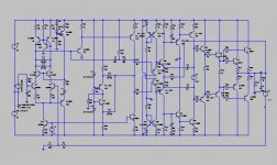
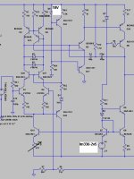
Here is the complete front-end design modified for a high degree of DC precision (minus supply rail decoupling and the input offset servo [to eliminate the need for a big decoupling cap]).
The important points are:
Temperature compensated and highly stable current sources are provided for the LTP tail and the VAS load.
The LTP tail current will be adjustable with a trimpot by a small amount, allowing the DC voltage across clamp diodes D2 and D3 to be trimmed out to 0.00X volts.
The VAS transistor has been cascoded. This is probebly the most important factor, as it allows the VAS transistor itself to be the same type at the three current mirror transistors and the VAS EF buffer. These transistors all dissipate very little power and Vbe variations (~2.2mV / deg C) due to transistor heating are practically taken out of the equation.
As a added bonus, the VAS cascode combined with the improved, cascoded VAS current source has significantly improved the front-ends linearity.
Cheers,
Glen
Attachments
And here are the simulation results for the compete amplifier.
THD-20kHz, delivering 80W into 4 ohms:
Harmonic Frequency Fourier Normalized Phase Normalized
Number [Hz] Component Component [degree] Phase [deg]
1 2.000e+04 2.527e+01 1.000e+00 -2.95° 0.00°
2 4.000e+04 9.730e-06 3.850e-07 -154.36° -151.41°
3 6.000e+04 1.716e-05 6.791e-07 -140.50° -137.55°
4 8.000e+04 5.647e-06 2.234e-07 -88.70° -85.75°
5 1.000e+05 7.052e-06 2.790e-07 48.49° 51.44°
6 1.200e+05 4.713e-06 1.865e-07 -113.36° -110.40°
7 1.400e+05 1.622e-06 6.419e-08 -167.06° -164.11°
8 1.600e+05 5.021e-06 1.987e-07 -105.92° -102.97°
9 1.800e+05 9.949e-07 3.937e-08 -67.10° -64.15°
Total Harmonic Distortion: 0.000090%
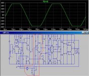
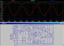
This is a worst case PSRR sim and this result was achieved using minimal supply rail bypassing and 1 ohm resistances in series with the power supply voltage sources (to induce huge amounts of ripple).
The attached plot show the output voltage along with the supply rail voltages.
The front end is powered from elevated voltage rails (6V higher) which float on top of the +/-42V rails for the power output stage.
All that was required to eliminate the Miller compensated VAS as a source of non-linearity, due to its reduced PSR at higher frequencies, was to add a basic capacitance multiplier to the positive rail of the front-end, along with a little supply rail bypassing.
The capacitance multiplier has an RC of only 1K/470nF and the emitter of the capacitance multiplier is followed with an RC of 10R/10uF.
The only bypassing on the negative rail of the whole amp is 10R/4.7uF.
The real life circuit will use capacitors larger than this by an order of magnitude or more, not to mention the fact that the impedance of the power supply will be a great deal less than 1 ohms at 20kHz.
Replacing the capaciatance mulitipler for the front-end positive supply rail with an ideal voltage source referenced to ground improves the simulated THD-20kHz from 0.000090% to 0.000077%, but if I tried to increased the 10uF bypass to 470uF to get the same results that way, I would have to let the simulator run for half a day.
Cheers,
Glen
THD-20kHz, delivering 80W into 4 ohms:
Harmonic Frequency Fourier Normalized Phase Normalized
Number [Hz] Component Component [degree] Phase [deg]
1 2.000e+04 2.527e+01 1.000e+00 -2.95° 0.00°
2 4.000e+04 9.730e-06 3.850e-07 -154.36° -151.41°
3 6.000e+04 1.716e-05 6.791e-07 -140.50° -137.55°
4 8.000e+04 5.647e-06 2.234e-07 -88.70° -85.75°
5 1.000e+05 7.052e-06 2.790e-07 48.49° 51.44°
6 1.200e+05 4.713e-06 1.865e-07 -113.36° -110.40°
7 1.400e+05 1.622e-06 6.419e-08 -167.06° -164.11°
8 1.600e+05 5.021e-06 1.987e-07 -105.92° -102.97°
9 1.800e+05 9.949e-07 3.937e-08 -67.10° -64.15°
Total Harmonic Distortion: 0.000090%
This is a worst case PSRR sim and this result was achieved using minimal supply rail bypassing and 1 ohm resistances in series with the power supply voltage sources (to induce huge amounts of ripple).
The attached plot show the output voltage along with the supply rail voltages.
The front end is powered from elevated voltage rails (6V higher) which float on top of the +/-42V rails for the power output stage.
All that was required to eliminate the Miller compensated VAS as a source of non-linearity, due to its reduced PSR at higher frequencies, was to add a basic capacitance multiplier to the positive rail of the front-end, along with a little supply rail bypassing.
The capacitance multiplier has an RC of only 1K/470nF and the emitter of the capacitance multiplier is followed with an RC of 10R/10uF.
The only bypassing on the negative rail of the whole amp is 10R/4.7uF.
The real life circuit will use capacitors larger than this by an order of magnitude or more, not to mention the fact that the impedance of the power supply will be a great deal less than 1 ohms at 20kHz.
Replacing the capaciatance mulitipler for the front-end positive supply rail with an ideal voltage source referenced to ground improves the simulated THD-20kHz from 0.000090% to 0.000077%, but if I tried to increased the 10uF bypass to 470uF to get the same results that way, I would have to let the simulator run for half a day.
Cheers,
Glen
Attachments
- Status
- This old topic is closed. If you want to reopen this topic, contact a moderator using the "Report Post" button.
- Home
- Amplifiers
- Solid State
- A superior VAS clamp and VAS current limit for the Blameless.