
Hi Doede and follow DDDac-builders.
Hope you have time for some small troulbeshooting questions 🙂
Some years ago a got a bag of old style DDDac main- and DAC-boards and some defective newer pcb's from another DDDAc-builder.
I assembled and repaired a secondary DDDac from an old-style MB's and two old-style DAC-boards. This deck have been running fine in my office ever since 🙂
Now i have got the "solder-itch" again and took a look inside the old scrap-yard bag. It still contains one old MB, one new MB, one old DAC-board and a new one.
I did mark the old DAC-board as "Right channel def." and the new DAC-board as "Both channel def." some years ago and I seems to remember both MB's were tested dead.
Now I started by reheated all solder pads on the two older boards and added a little new solder. I then carefully examined both boards visually and checked the most obviously connections.
All good... I then connected the DAC-board and heard... nothing!!! Now I checked every connections without finding any problems.
All LDO's give correct voltage, BCLK and LRCLK connections are intact from I2S entrypoint up to the DAC-boards. GND is fine everywhere.
DATA is good from I2S entrypoint to first 74VHC164MX-chip (pin 1 and 2) and all connections between these 5 74VHC164MX seems fine as well as the exit-points for R- and L-channels and up to the DAC-boards.
Now I removed all I2S (and GND) wires for both channels from MB and up the the DAC-board and connected new wires (about 5-6cm long) directly from the top connection-points on a functional DDDac and onto the top connection-points of the defective stack...feeding channel separated I2S directly into the old DAC-board bypassing its own MB. Music were now playing from both channels!!!
So... the old DAC-board seems now completely fine (after reheating) and the power distribution on the old MB as well as the the analog side also seems fine.
Conclusion!!! the I2S DATA line is nonfunctional on the old MB. If the problem isn't a defective connection, and I don't think so, it most be one or more 74VHC164MX-chips which have failed.
Since the Right-channel breaks out after the first 74VHC164MX-chip, this chip seems a logical point of failure. Of cause more chips could be defective as well.
Do you agree on this conclusion or have I missed another possibility?
Are there any "clever" ways to check the 74VHC164MX-chips health before replacing them ?
...and sorry for the long post.
Regards
Martin Roerup, Denmark.
So you ran the early red board with the new dddac DAC module? That would probably fail
the new MB have a 74 flip flop to delay half A clock cycle. The first generation dac Modules and red boards did not have this. In stead there was a 1kOhm resistor in series with data to create this delay.
so in stead of using a wire from MB to DAC board for the DARa line, install a 1kOhm resistor and see what happens. As said only when the MB is the old red one and the da. Module is of newer generation
No no... ALL boards involved here are old style MB's (Red) and old style DAC-boards (without Tent shunts). Two old DDDacs... one functional deck and one defective deck.
I used my perfectly functional deck with two old-style DAC-boards on top to "inject" a known working L/R channel separated I2S-signals directly into the other problematic decks DAC-board which I'm trying to troubleshoot.
By doing this I bypassed the problematic motherboards own I2S processing completely (from the I2S input socket, through the 74VHC164MX-chips).
Doing this test I still uses the problematic old-style MB's 12V power handling to the DAC-board as well as the analog output from the 1794's through the I/V resistors and out.
This test works fine with music now playing from the defective deck... although with L/R I2S comming from the functional deck. In my logic it proves that this DAC-board also works fine and the problem is the defective decks motherboards I2S logic.
Since these motherboards are rather simple it leaves one or more 74VHC164MX-chips as the only possible failure points, since I have checked all PCB-traces and voltages.
So my questions are...
Is my logic flawed here? ...and can I test the 74VHC164MX-chips health without first replacing them?
Ok, understand, in that case I would measure the integrity of the I2S signals at the input of the DAC deck coming from both red boards to compare. Do you have an oscilloscope to do this ?
Well no... but I'm considering buying this fellow: OWON VDS 1022i on Amazon.de for about €125
It might be both cheaper and easier just to start replacing the 74VHC164MX-chips, but I might learn much more by going for the oscilloscope.
...and to be honest, the learning part of this repair project is actually a large part of the experience. It's not that I really neeed a third (or maybe even a fourth DDDac ;-)
...and to be honest, the learning part of this repair project is actually a large part of the experience. It's not that I really neeed a third (or maybe even a fourth DDDac ;-)
Hello, my first post here.
I remember a discussion in this tread about possibile benefits by replacing standard Wima 100nF bypass with Kemet 68nF (even if I not remember which positions should be replaced, I'm not able to find the original post).
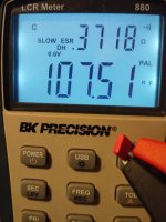
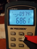
Today I measured both capacitors ESR at 100KHz using an LRC meter and result is Wima ESR=0.370 ohms and Kemet ESR=0.098 ohms.
Sorry for my question, I'm a Newbye in electronic : is the lower ESR the main reason of reported overall benefits ?
Thank you.
Max
I remember a discussion in this tread about possibile benefits by replacing standard Wima 100nF bypass with Kemet 68nF (even if I not remember which positions should be replaced, I'm not able to find the original post).
Today I measured both capacitors ESR at 100KHz using an LRC meter and result is Wima ESR=0.370 ohms and Kemet ESR=0.098 ohms.
Sorry for my question, I'm a Newbye in electronic : is the lower ESR the main reason of reported overall benefits ?
Thank you.
Max
Attachments
Finally I have my DDDAC up and running again🙂 there is one issue that arises with the balanced output. If I use balanced output without caps to my amp, all seems fine. Except I don't feel comfortable using it this way (dc still present).
So I add caps in series on pos and neg and connect pos and neg via XLR to amp. When I use caps, I have a weird noise upon amplifier shutdown that is not present in the capless situation. Any pointer as to what that could be? I tried parallel 150k resistors from caps to gnd pin of XLR, but that did not work.

So I add caps in series on pos and neg and connect pos and neg via XLR to amp. When I use caps, I have a weird noise upon amplifier shutdown that is not present in the capless situation. Any pointer as to what that could be? I tried parallel 150k resistors from caps to gnd pin of XLR, but that did not work.
You should not let the main power wires go that close to the signal cable.
I would also not suggest in general to connect pin 1 to the DAC gnd. only Chassis / mains Safety ground.
on the weird sound, i guess this is a discharge kind of thing. may be as Caps are not 100% identical?
on the weird sound, i guess this is a discharge kind of thing. may be as Caps are not 100% identical?
Known PIN1 issue. When I had capacitors on the output (Jantzen Silver Z 4.7uF 2%), there was some small noise when switching off, this is probably unavoidable. There is no such thing with a transformer. As for Pin 1 ground, I tried tying it to both signal GND or chassis, I didn't notice any difference in use. The signal GND is connected to the chassis indirectly, using GREC+100nF+100ohm. By default, Pin1 connects the chassis of two balanced devices, DDDAC and Preamplifier/Amplifier. XLR cable shield is also connected to the chassis. If Ground Loop occurs, Pin1 and shield should be disconnected, but only on one side, it must be grounded somewhere.
Thanks all,
This is still my "testbed" trying different things, LT3042 regulators, adding a second board, looking forward to that! Adding Iron Pre as buffer. I will reroute power lines as this indeed might influence results🙂
As for pin1, it is grounded at amp side.
I will try as suggested in documentation though:
I would like to improve FifoPi J5 psu. Now, I found below drawing of Doede:

In my situation I want to feed FifoPi J3 with Ultrabib shunt at 5V and then add RC filter plus LT3045 regulator to J5 (3.3V).
For the RC filter I ordered 162R resistor and accidentally 4700uf capacitor instead of 47uf.
What would be the workable value for the C in the above mentioned RC filter?
Thanks!
Robin, please have a good look what I did with the RC filter. The 165 Ohm is reducing the input voltage to the LT3045 to reduce power dissipation. The value is totally depending on the voltage drop from the 12V PSU to 6 volts input. Reason being is, that the current drawn by the Fifopi clock side is also dependent on the type of XO clock, as well on which FS frequency the track is playing. The value of 165 was measured in this very particular case ! With Accusilicon by the way.
so in summary, I would use the 5 volt regulator followed by the LT3045 and not use a RC filter unless you can make it totally specific to your application
so in summary, I would use the 5 volt regulator followed by the LT3045 and not use a RC filter unless you can make it totally specific to your application
Oh yes, now I recall, I intended to use the ultrabib that feeds the DDDAC mainboard (12v) so then the RC would make sense, as I have Accusilicon so expect the same mA draw.
Thanks for the explanation though, as I aim to use 3.3v and not 6v😉
I will proceed without RC.
Thanks Doede!
Thanks for the explanation though, as I aim to use 3.3v and not 6v😉
I will proceed without RC.
Thanks Doede!
Doede, or somebody, please clarify something to me.
If I connect FifoPi Q7 and DDDAC through SCK/LR/SD, how is it possible to clock the DDDAC with Q7's clock?
If your answer is that SCK/LR/SD carry the clock, then why does Q7 have MCLK output?
It confuses me a lot.
If I connect FifoPi Q7 and DDDAC through SCK/LR/SD, how is it possible to clock the DDDAC with Q7's clock?
If your answer is that SCK/LR/SD carry the clock, then why does Q7 have MCLK output?
It confuses me a lot.
- Home
- Source & Line
- Digital Line Level
- A NOS 192/24 DAC with the PCM1794 (and WaveIO USB input)