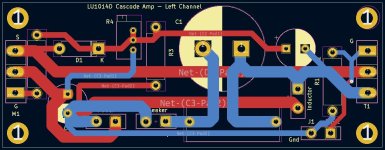
I am not sure that a discrete star ground is better than a star ground that incorporates a ground plane. In my "star ground", the layout would have been the same regardless of discrete ground traces or ground plane. The only difference would be that with a ground plane the ground connections would be within the ground plane and the electrons would flow according to their return paths. That has worked so far in my amplifier PCBs because I was able to route the circuit efficiently on the top layer with only a few short traces or no traces on the bottom layer. The ground plane was not broken up so the ground return paths were not impeded by traces.
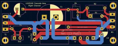
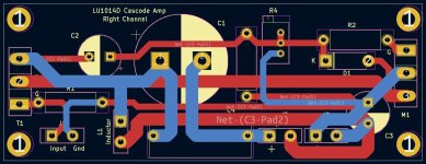
Modified the right channel PCB slightly to tighten the inductor return path for a smaller loop.
My reasoning for the star is to keep the high currents from the inductor separate from the other ground paths. It's probably ok to combine the other ground traces.
My reasoning for the star is to keep the high currents from the inductor separate from the other ground paths. It's probably ok to combine the other ground traces.
Attachments
I think I'm getting close to the final version of the PCBs. On the left channel PCB, I've added a jumper in place of the trace from the input pad to the JFET gate in order to avoid a long circuitous route. Also, the MOSFET gate resistor has been moved to shorten the trace to the gate connection. Some other small changes, as well, were made to tighten things up.
Attachments
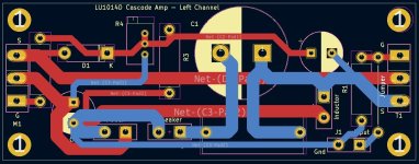

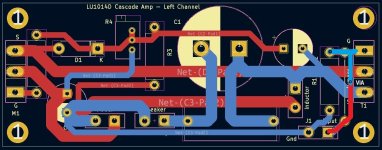
I thought about using a via but I couldn't see a route. I had been working on these PCBs for too long and wasn't seeing straight. Thanks, Ben. I'll give it a try.
I've implemented Ben's suggestion and replaced the jumper with a via and traces. I think I'm done with these PCBs, so I'm going to take a break from this, and tomorrow I'll generate the Gerber files and place an order.
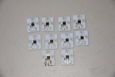
My last order for PCBs arrived from JLCPCB just now. These are the LD1014D breakout aluminum PCBs. I ordered them on June 23rd, and here they are on July 4th. Pretty quick turn around. Now, I can solder a bunch of SMDs and do some curve tracing.
My last order for PCBs arrived from JLCPCB just now. These are the LD1014D breakout aluminum PCBs. I ordered them on June 23rd, and here they are on July 4th. Pretty quick turn around. Now, I can solder a bunch of SMDs and do some curve tracing.
Attachments

Yes. I will make the Gerber files available after I have tested them.
I placed my order for amp PCBs to JLCPCB on June 5 and they are at their shipping centre today ready to go out. I paid for the cheapest delivery so they should be here in10 days or less.
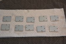
Meanwhile, I did some work on soldering the LD1014Ds to the adapter boards. Looking at the back of the PCBs, I noticed that there were raised edges (burrs) at the board perimeter and holes. Not huge, but if I dragged a finger nail across it, I could feel it. So, I used 600 grit sandpaper and a flat surface remove the burrs.
After doing the sanding and seeing the results, I was wondering if the boards were flat. Luckily, I have a dial gauge mounted on a flat chunk or granite (I think) that I could use to check for flatness. After some measurements, I found the removed areas at the board corners are actually about 1/1000 inch thinner and the boards are basically flat. So, the uneven sanding was the result of my poor technique, not because the boards are concave. A little sanding to remove the burrs is all that is needed.
I used the cast iron fry pan on electric stove burner method for reflowing the SMDs to the adapter boards. I've never done this before, so I did one first and did a quick curve trace on my Arduino Frankentracer. I was happy to see that the reflow was successful. Three batches of three boards followed and now I have 10 LD1014Ds mounted on PCBs.
I did not solder terminal pins for the LD1014D to the PCBs. I am going to hand solder short segments of solid 18 gauge wire to the PCB pads. These will be bent at right angles for insertion into the amp circuit board. I did that for the first board for curve tracing..
Next, I will curve trace the LD1014Ds for testing and matching.
Attachments
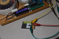
I was thinking about how to simplify my curve tracing task. Originally, I was going to solder leads to the pads of the PCBs but the more I thought about it, the less attractive the idea became. A lot of work and not pretty. However, I will still solder wires for my build because I like a secure connection.
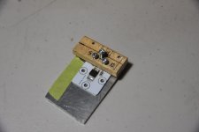
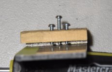
So instead, I came up with the plan of building a test jig to make reliable contacts with the PCB pads and be relatively quick to connect and disconnect. Luckily, I have all sorts of scraps from my projects to provide building materials. Some aluminum plate and wood were used to make this jig. I tapped 4-40 screw holes in the wood and hardened the threads with white wood glue. The wood is not ideal for this, but for a small number of uses, it will work. If I was testing a large number of devices, I would replace the wood with a thick piece of plastic.
Some steel 4-40 screws are used to clamp down the PCB and to make contact with the PCB pads. The screw heads are perfect for clamping onto with alligator clips.
Sometimes, being lazy is a good thing.
Attachments
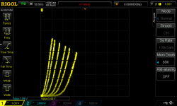
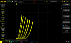
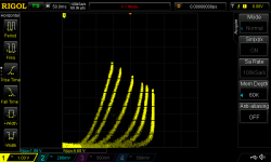
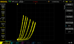
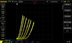
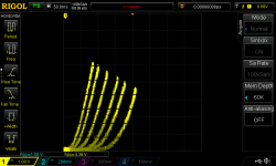
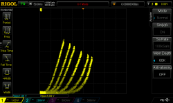
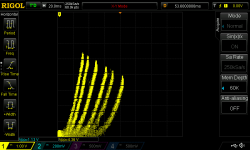
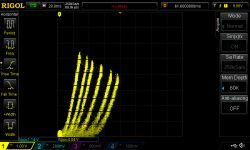
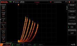
I traced the LD1014Ds today. Out of the 10 devices, two were defective. One traced as a short while the other acted as a resistor. I reflowed one with hot air but it didn't make any difference. I removed the bad devices from the PCBs and I will reflow new ones to the boards.
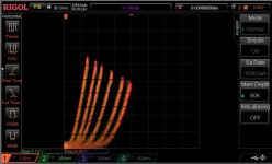
Vgs started at -0.9V and stepped at -0.1V.
I was surprised at how quick the tracing went. From start to finish was about 30 minutes. I'm glad I built the Arduino/Frankentracer.
Vgs started at -0.9V and stepped at -0.1V.
I was surprised at how quick the tracing went. From start to finish was about 30 minutes. I'm glad I built the Arduino/Frankentracer.
Attachments
-
 DS1Z_QuickPrint8.png15.1 KB · Views: 81
 -
 DS1Z_QuickPrint7.png15.7 KB · Views: 84
 -
 DS1Z_QuickPrint6.png16.9 KB · Views: 82
 -
 DS1Z_QuickPrint5.png16.3 KB · Views: 81
 -
 DS1Z_QuickPrint4.png16.3 KB · Views: 78
 -
 DS1Z_QuickPrint3.png16.1 KB · Views: 77
 -
 DS1Z_QuickPrint2.png16.1 KB · Views: 75
 -
 DS1Z_QuickPrint1.png16.6 KB · Views: 79
Yes. The uneven spacing produces the 2nd harmonic. My test amp, though, shows the distortion to be fairly low. Low enough for me, anyways. My other SIT amps have higher distortion and I'm fine with that.
For this build, I'm going to keep it simple without feedback. However, I've got so many LD1014Ds that I'm sure another amp is in the future. That will be a good time to try different things.
For this build, I'm going to keep it simple without feedback. However, I've got so many LD1014Ds that I'm sure another amp is in the future. That will be a good time to try different things.
I repopulated the two failed PCBs with new chips and they traced out good. As a bonus, these new ones each matched up well with a device from the initial batch.
Attachments
When I matched the Pass Stash multi-hundred lot, I matched them at the bis voltage and current and I measured gain (delta Id/ delta Vg) at that bias point.
I also measured Vpinch of every part.
How good the match is depends on how many devices you measure. At 300 pcs, almost all parts matched well. If I remember, the matches started happening well at around 100 pcs.
I also measured Vpinch of every part.
How good the match is depends on how many devices you measure. At 300 pcs, almost all parts matched well. If I remember, the matches started happening well at around 100 pcs.
I've been trying out a couple of LU1014D LTspice models which I have found on this forum, and they have been doing funny things. First, I have not been able to produce reasonable curves using LTspice. Second, when modelling my amp design, I found that varying the gate voltage of the cascode MOSFET does not change the current through the system. The LU1014D's Vds changes but the current varies by only a very small amount.
So, I decided to use Michael Rothacher's SIT Modeller with one of my LD1014D traces (#2) to produce my own LTspice model. I managed to accomplish that after some fooling around. The modeller had trouble with a low Vds range so I expanded the JPEG to include a Vds range of 32 volts. After doing this, I managed to produce a set of curves that were close to the traces.
I used LTspice to generate some curves for comparison with the traces, and the results are in the ball park. Next, I ran some amp simulations where I varied the gate voltage to the cascode MOSFET and that produced changing current with Vds.
Here is the LTspice model for those who may be interested in trying it out;
*--------------------------------------------------
*LU1014D
*GENERATED BY SIT MODELER @ PASSDIY
*MODEL RANGE: 32V, 1.6A
*--------------------------------------------------
.SUBCKT LU1014D D G S ; Drain Gate Source
+ PARAMS: MU=8.34 X=9.61 K=0.09 N=0.09 VCT=1.91 RG=2MEG
*--------------------------------------------------
B1 D S I=K*PWR(URAMP((V(G,S)+VCT)+(N*LN(V(D,S))+(V(D,S)/MU))),X)
FOR MULTISIM COMMENT OUT ABOVE LINE () AND UNCOMMENT NEXT LINE
*B1 D S I=K*PWR(MAX((V(G,S)+VCT)+(N*LN(V(D,S))+(V(D,S)/MU)),0),X)
R1 G S {RG}
CGS G S 784P
CGD G D 363P
CDS G S 0P
.ENDS LU1014D
*--------------------------------------------------
Thanks to @Michael Rothacher for the great tools (SIT Modeler and Frankentracer).
Attachments

- Home
- Amplifiers
- Pass Labs
- A Low Power Cascoded LD1014 Choke Loaded Source Follower