It's summer and it's getting hot in this neck of the woods, so I've either got to stop listening to my music or reduce the heat output of my system. My air conditioning system is limited because I have hot water heating in my house so I can't easily install central air conditioning. I make do with a portable in-room unit. Well, I'm not going to stop listening to music, so I've got to reduce the heat from my system.
Yesterday, I changed from my multi-amped JBL speaker system to my Quad ESL speakers which reduced my amp-produced heat by one half. But there is still significant heat output, around 150 watts, although less that the 350 watts or so with my JBL system.
So, I thought, I need a lower powered class A amplifier. I also needed to feed my amp building addiction. I remembered that I had bought a whole bunch of LU1014D power JFETs a while back and they were just sitting around gathering dust. After some research, which included reading Nelson P's Zen Variations 8, I decided to build my take on the cascoded JFET amp.
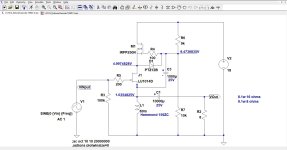
I am hooked on source followers, so I fired up LTspice and modeled a choke loaded cascoded source follower. After a bit of fiddling around, I found that such an amp with 18V power supply could produce about 8 or 9 watts into 8 or 16 ohm load and only dissipate about 25 watts, at least in theory. This would be enough power for my speakers and not too much for my air conditioner.
Next, I searched through my stash of parts and and managed to find my power JFETs. Unfortunately, they are the SMD variety (LD1014D) and that makes things a little more difficult for my old eyes. Probably that's why I got 50 of them for almost nothing. Now, generally you get what you pay for, so I needed to curve trace one to see what I actually had in my hands.
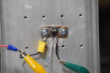
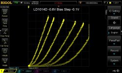
After much fumbling around (breaking the legs off one device, and one ran away and hid somewhere), I managed to solder one to a small piece of copper and attach wires to the gate and source pins. This was mounted to a heatsink, and I produced some nice triode-like curves on my Arduino/Frankentracer system.
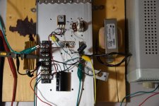
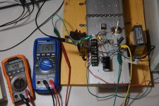
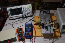
To make a long story short, I assembled a prototype amp over the last couple of days and I fired it up (without fireworks) today and did a quick distortion measurement. I used my Victor oscillator as the source and I could only coax about 6.5Vpp out of the amp due to the limited output of the oscillator, but the results are encouraging.
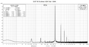
With 18V power supply, I measured about 0.67 watts out into an 8 ohm resistor. After playing around with Vds, I managed to get THD to about 0.033%. Again, this 0.67 watts is the maximum that I could get with the limited output voltage of the oscillator. LTspice says the amp will produce 8 to 9 watts, but we'll see. I will use my modified Luminaria preamp (choke loaded) which can swing quite a bit of voltage at low distortion next to see what the power limits of this amp are.
Attachments
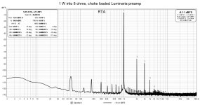
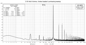
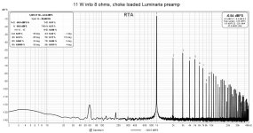
I used my choke loaded LuminAria today to drive the LD1014 follower and measured the outputs at 1W, 3W, and 11W. The LD1014 operating point was kept the same as yesterday at 4.84 Vds and 1.84 A.
Interestingly, the 1 W output shows lower distortion than the test at 0.67 W from yesterday. Maybe some distortion cancelling? The amp managed to put out about 11 W into 8 ohms with 0.5% THD. The distortion profile shows higher 3rd harmonic with the LuminAria in the chain.
Interestingly, the 1 W output shows lower distortion than the test at 0.67 W from yesterday. Maybe some distortion cancelling? The amp managed to put out about 11 W into 8 ohms with 0.5% THD. The distortion profile shows higher 3rd harmonic with the LuminAria in the chain.
Attachments
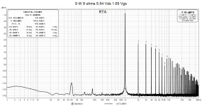
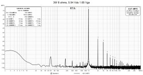
I experimented with changing the Vds of the LD1014 by adjusting the value of R6 which affects the bias of the IRFP250N. With 5.54 Vds and 1.65A, the distortion profile show less 3rd harmonic. The total distortion rises a bit and the maximum power output goes down a little to about 9W at 0.5% THD. I can live with that.
I think this design will do what I want, so I'm proceeding to the PCB stage. I've already got some preliminary layouts.
I think this design will do what I want, so I'm proceeding to the PCB stage. I've already got some preliminary layouts.
Attachments
There is a metal substrate adaptor pcb design floating around the forum somewhere designed for the Ld1014.
XRK designed iirc.
It neatly converts the smd part into something like a to-220 with a source resistor and a header for easy wiring.
To difficult to find from my phone browser but it shouldn't be too hard to find from a desktop.
XRK designed iirc.
It neatly converts the smd part into something like a to-220 with a source resistor and a header for easy wiring.
To difficult to find from my phone browser but it shouldn't be too hard to find from a desktop.
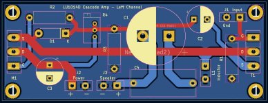
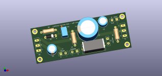
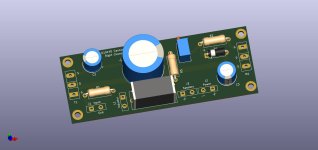
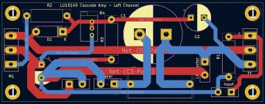
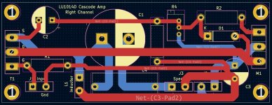
I have finished the PCB designs for the left and right channels and power supply filter in KiCad. The amp boards are 100mm x 38mm, and the power supply CLC board is 127mm x 26mm. I just need to do some final checks on each, and then it's off to the fabricator.
Attachments
Sorry, ZM. You'll have to be a little more specific. I'm still a rookie at PCB design. Any advice is welcomed.
Yeah, it just occurred to me that is what he was referring to. I did increase the width of the spokes in consideration of the current. I can change to solid pads. I have a large soldering iron just for high heat use.
It seems most amplifier boards that I have seen do not have ground planes so thermal reliefs are non-issues. ZM does use large copper pours and no thermal relief for power connections so more heat is required.
Being a rookie at PCB design too and a diyer with no formal electronics education who is just winging it, I have also put ground planes in my PCBs. I did some checking with an online PCB trace calculator and the thermal reliefs in the boards that I have done have more than enough capacity, even assuming only a 1 degree C rise in temperature, for the 3A maximum that I expect in my boards. I do not anticipate the spokes to act as fuses.
I noticed that your schematic showed a gate resistor at the LU1014D and the PCBs do not have one.
Also your left channel board has the input pads located on the opposite side of the board from the power input. That makes the route for Input ground to power ground rather circuitous. Locating the inputs at the same side of the board as on the right channel board would be much better.
Ground planes are more correctly employed in digital circuit boards, where switching speeds are in the MHz or GHz ranges. In these types of boards, there will often be a digital power plane as well, and the power and ground planes will occupy the the two innermost layers of a multilayer (4+) PCB.
Audio frequency boards are best with more of a star grounding layout. Heavy traces are run from a common connection point to the places where active devices and decoupling capacitors are located. With relatively heavy current designs, the ground connection between the PSU board is best tied into a single point on the channel board. The speaker negative connection may be connected adjacent to this point, but is usually best when connected as close as possible to the terminals of the bulk bypass capacitors on or next to the PSU.
Audio frequency boards are best with more of a star grounding layout. Heavy traces are run from a common connection point to the places where active devices and decoupling capacitors are located. With relatively heavy current designs, the ground connection between the PSU board is best tied into a single point on the channel board. The speaker negative connection may be connected adjacent to this point, but is usually best when connected as close as possible to the terminals of the bulk bypass capacitors on or next to the PSU.
In my boards, whether PCB or veroboard, I always place the power in and power ground, speaker out and speaker ground, and bypass capacitor all very close together. I like to keep loop areas as small as possible. Basically I try for a "star ground" at the power input/decoupling capacitor point of the amplifier board. It has worked well for me so far. I hear no noise from my 103dB speakers.
These are all great comments. Thanks. I'm going to rework the PCBs.
The gate resistor for the LD1014D is located on the separate LD1014D PCB.
The gate resistor for the LD1014D is located on the separate LD1014D PCB.
Another thing that you can do to maximize the ground connection is to join the power ground with the speaker ground with a wide trace on the top layer, and connect the trace to the bottom plane with vias. I did that on my THF-51S Mu Follower Follower board. The same can be done with the inductor ground. You can also connect the inductor ground to the power ground and speaker ground on the top layer. It is a straight run.
- Home
- Amplifiers
- Pass Labs
- A Low Power Cascoded LD1014 Choke Loaded Source Follower
