usual way, when adding optional components, is to arrange them in schematic file in additional pages, so not present of main schematic page
I amn't sure that i understood well...
Parallel parts can't represent two channel configuration.
Different link spacing is another story.
Parallel parts can't represent two channel configuration.
Different link spacing is another story.
Last edited:
well, it depends of pcb software, in fact, but practically any bigger commercial software package is having that option - multiple schematic pages, you can put whatever you want on them, and inter-page connections are sorted either by trace names or flags
example - I'm doing my pcbs in good old Eagle 6.3
say Babelfish M25 - channels are sort of mirror image
schm. one page one channel, schm. second page second channel
Edcor autoformer shown on each channel
optional Jensen and Cinemag autoformers placed on 3rd schm page
so, no confusion - at least not about these parts
anyhow - I remember at first, 'till I didn't figure out that way, I did draw optional parts (say different size of caps and resistors) on same schm. confusing heck of my self

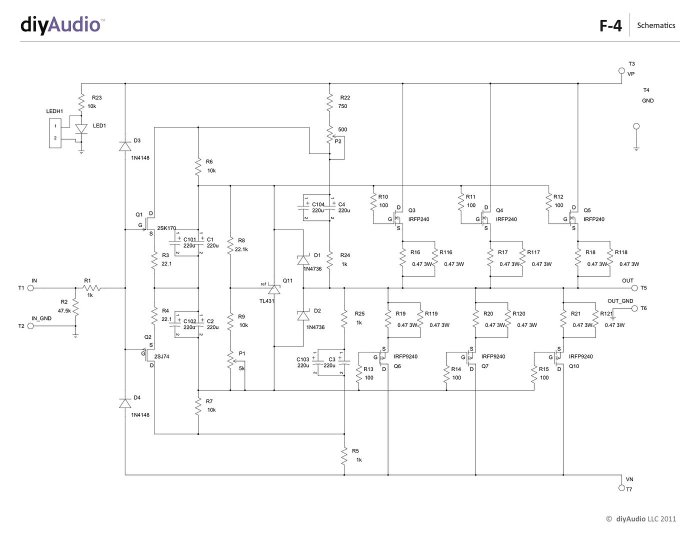
Question on the purpose of R24 and R25 in the F4 schematic. C3&4 provide a bootstrapped voltage for the input jfets and it would appear that R24 and R25 effectively just add ESR to C3&4. Wouldn’t it be better to directly couple C3&4 to the output for a more stable power supply for the jfets? Essentially make R24&25=0. Perhaps R24&25 were intended to be in parallel with C3&4 to cut down the voltage applied to the jfets? Looking for one of the EE’s out there to comment.
Thanks!
Thanks!
Without those resistors the voltage of the insides of capacitors C3 C4 would be tied completely to the output, those resistors bootstrap the caps so the voltage on the Jfet can bounce a little high than the rail when needed.
Thanks 6L6 for the response. I thought those caps charge through R5, P2 and R22. At idle they charge to roughly 24 volts and then effectively low pass filter the voltage difference between the output and the power supply rails to bootstrap above the output. Very long time constant makes them kinda like a battery floating above and below the output. Hence R24&25 aren’t needed as they just add 1k of power supply impedance to the jfets. What am I missing?
ref to re-linked schematic from first post (down)....
imagine R24 on top of C4, and R25 on bottom of C3
maybe then it's clearer - as I see it - with additional 1K, Pa made bootstrapping somewhat more compliant
additional resistance is resulting in slower discharge of said caps (in large signal circumstances); charge too, but let's believe that he did optimize it that way
I never did any testing to determine is it better that way, but with years I did learn that his detailing is always having a proper purpose
If nothing else, I know that (even) he's also finding pleasure in gilding the Lily; it's his Lily, in first place
Thanks for inputs. What I’m picturing is that R24&25 effectively act as passive mixers of the bootstrap voltage from the output with the bias voltage coming through R22+P2. Roughly the same 1k source impedance of the two voltages so that they add equally.
What I am concerned about is the amount of noise on the jfet power supply showing up on the output. A measurement of a DIY F4 on the Super Best Audio Friends website showed a lot of power supply noise on the output and I would like to reduce this. Not clear to me how much of this noise is coming through the MOSFETS vs the jfets. Ideally a PSRR modeling in Pspice would answer this.
I’m thinking that if I added a capacitor from the drain of jfet Q1 down to the drain of Q2 I would still be allowing the passive mixing of the two voltages but greatly reduce the power supply noise across the jfets.
Thoughts?
Rather than altering the circuit as designed and intended, I would take a look at the main power supply in general. Perhaps changing to a CLC rather than a CRC if that is what's there now. Maybe more capacitance, particularly at the second "C" position. Could go CRCC there, as an idea.
Yes, I am using a fairly large CRC supply with (8) 33,000 uF caps. I’ve also used CLC. Pretty beefy for a brute force analog supply.
I put a scope differentially across the jfet drains and indeed see the power supply ripple (~4mv) at idle as expected. DC voltage about 27 from drain to drain. All as expected. With music playing the power supply noise signal becomes mixed with audio signal as expected with the passive mixer of bias and bootstrap signals. Ideally for lowest distortion and noise from a source follower circuit I’d like to see constant voltage gate to drain. I tried adding a 100 uF cap jfet drain to drain and it worked well. The drain to drain DC voltage stayed fairly constant even with the amp driven hard. I could no longer see any ripple voltage drain to drain with my oscilloscope. I don’t have any great tools to measure PSRR or distortion to verify any signal improvements, but from a jfet power supply noise perspective this looks like an improvement. Super easy to implement without removing boards, just tack solder cap from top of R6 to top of R7.
As a side note I also am using Exicon laterals with no source resistors and a LMV431 in place of the TL431 to enable lower bias voltage adjustment range for the laterals. If there is interest, I’ll post schematic and photos. Not sure if it belongs here or the F4 forum for comments.
Not sure if it belongs here or the F4 forum for comments.
it is F4, sort of
Since I was playing around with some amps, I took the occasion to connect my F4 after quite a long while (a year maybe). This lil' beast's transparency and ease is just absolutely fantastic.
It’s genuinely special, every builder should make one.
- Home
- Amplifiers
- Pass Labs
- A guide to building the Pass F4 amplifier