Member
Joined 2009
Paid Member
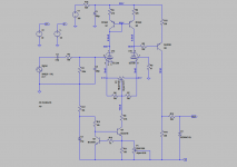
Why MJE350 is not emitter follower? Wouldn´t it be better to have lower impedance drive for the IRF530?
I would (wildly) guess that it's done this way because it provides for better PSRR because it appears somewhat of a variation of the Taylor follower.
Hi, Valery
I've been following your thread.
As soon as Terry gets boards I'll contact him to see if he is willing to sell me a set of boards.
I'm to eager to follow his build a well.
I have new old stock of those tubes and tube sockets for them,
I'll have a closer look to see what power transformers will be needed
Regards
OK, cool 😉 Let me know if you will have some questions

Would it be possible to implement modulated CCS like in Pass´s Aleph amplifier for the IRF530 VAS?
IMO, Alephs are single ended while this IOTA-CD is push pull. The 9530 and 530 feed the 1.2R base bias resistors to a push pull amplifier.
Why MJE350 is not emitter follower? Wouldn´t it be better to have lower impedance drive for the IRF530?
That 360R resistor, while it's awkward value for E12 resistor series, really has to be kept at that value because it provides the bias to the MOSFET's Vgs. Any lower, MOSFET might not turn on and any higher, MOSFET will be biased too hot. I don't see how to make an emitter follower at 11mA of current with 360R as emitter resistor while the base is somewhere at 97 volts. Others will have to correct me.
Member
Joined 2009
Paid Member
IMO, Alephs are single ended while this IOTA-CD is push pull. The 9530 and 530 feed the 1.2R base bias resistors to a push pull amplifier.
That's my take on it too, after all, just because the feedforward Class A amplifier is single ended does not make it a SE amplifier (except at sub watt power levels where the current dumpers remain silent).
I don't see how to make an emitter follower at 11mA of current with 360R as emitter resistor while the base is somewhere at 97 volts.
You'd have to shift ground reference and have a B- for the cathodes instead of a B+ for the anodes. I don't see any benefit of doing that and like the design as-is.
I'm working on a hybrid power amplifier with a tube front-end and MOSFET output stage using a design very similar to the IOTA-CD circuit shown in the original post, so I simulated the input portion of this circuit in LTspice to get a sense for how my own design might work. I've attached the partial IOTA-CD circuit simulation files here.
In my simulations, the DC voltages on the plates of the ECC88 input tubes (and the collectors of their corresponding BC640 current mirror transistors) latch at close to the positive supply rail as indicated in the graphic. Of course, this condition only allows the plates to swing a few volts positive before being clipped. I haven't built a prototype to verify this behavior in an actual circuit, and have no doubt that the design works as Dr. Jagodic claims, but can anyone explain what is going on with the input stage, or point out what may be wrong with my SPICE simulation?
Thanks.
Attachments
Last edited:
Member
Joined 2009
Paid Member
I could be wildly out here - but if you look at the datasheet, for a 5mA cathode current the tube 'wants' to see 80V or os on the plate-cathode. So if you want the plate voltage to be lower you'll need to reduce the current.
I could be wildly out here - but if you look at the datasheet, for a 5mA cathode current the tube 'wants' to see 80V or os on the plate-cathode. So if you want the plate voltage to be lower you'll need to reduce the current.
While that is true, the plate also needs to swing above and below its quiescent voltage. There is almost no headroom between the idle plate voltage and the high voltage supply, which limits how high that voltage can rise.
I modeled the entire amplifier and you do get a clean sine wave output up to about 40 volts peak, but this seems to be a result of feedback. The waveform at the plate of the tube is quite distorted (at least, in simulation).
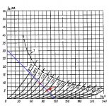
Do you need a lot of swing on the plate voltage? The way i see it, you only need to swing a few volts, just enough to drive the VAS which does most of the amplification. On ANUBIS thread, i did something similar.. The difference is that my B+ for tube is 120V and i use 3K9 for load resistors (no current mirror). Based on the load line chart, it has quite a swing as you can see on the attachment.
Also, 5mA is a bit low of ECC88. It won't be quite linear at that current. I got mine to idle at 7.7mA at B+ of 120V for the lowest offset on the output. That's around 90V on the plate.
edit: i use 6N23P instead of ECC88 but they're quite similar.
Also, 5mA is a bit low of ECC88. It won't be quite linear at that current. I got mine to idle at 7.7mA at B+ of 120V for the lowest offset on the output. That's around 90V on the plate.
edit: i use 6N23P instead of ECC88 but they're quite similar.
Attachments
Last edited:
Do you need a lot of swing on the plate voltage? The way i see it, you only need to swing a few volts, just enough to drive the VAS which does most of the amplification. On ANUBIS thread, i did something similar.. The difference is that my B+ for tube is 120V and i use 3K9 for load resistors (no current mirror). Based on the load line chart, it has quite a swing as you can see on the attachment.
I've been doing primarily tube designs for the past several years and am just getting back into solid state circuits. The operating point you've shown is typical of how I bias tubes as well, placing the operating point near the center of the load line so that the plate signal can swing approximately the same amount in both directions before clipping. I also try to make sure that the driver stages do not clip before the output stages so I'm generally looking for lots of headroom in the front end stages. But maybe this isn't as important in solid state circuits? Any insights from the solid state experts would be appreciated.
Member
Joined 2009
Paid Member
SS doesn't often clip gracefully, especially when nfb is used. In a hybrid there may be some benefit in having the tube stage control the clipping behaviour.
I have a hybrid amplifier circuit what I would love to build in the near future.
Some people built it with excellent result (Hungarian forum).
Can I post the schematics here?
Greetings
Some people built it with excellent result (Hungarian forum).
Can I post the schematics here?
Greetings
Member
Joined 2009
Paid Member
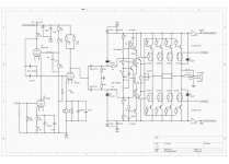
OK here we go
I didn't ask permission if I can share the circuit here, I hope I do not run into problem.
These is a Hungarian DIYaudio site.
audiodiyers.hu • Téma megtekintése - Hibrid er?sít? bipoláris tranzisztorokkal nvcs nélkül
You can see a lot of detail there, lot of pictures, unfortunately is Hungarian..
But the circuit is international language ha ha ha😀.
Attachments
I have a hybrid amplifier circuit what I would love to build in the near future.
Some people built it with excellent result (Hungarian forum).
Can I post the schematics here?
Greetings
Please do.
This is the first time I have seen this thread. The design in the original post is beautiful. 🙂 I've been thinking about something like this for a long time.
Member
Joined 2009
Paid Member
Hi Gaborbela,
Looks very interesting!... with no GNF it will have more of a tubby sound I think.
The OPS:
It has some features I'm not familiar with. You have a triple with 3 pairs which feeds the speaker through an inductor - which is good because it keeps the impedance of the OPS high for the tube stage. But you have a 4th pair of output devices which feeds the speaker through a resistor - what is this for ? and you hint at a protection circuit ?
The Vbe multiplier has a bias string made from 68k resistors to each rail. Perhaps there is no need for anything different but I wonder if there is a benefit in using bootstraps instead. This would mean replacing each 68 k resistor with a pair of resistors and then connecting the midpoint of each pair to the output with a 100uF capacitor ?
Maybe the base stoppers on the output devices could be smaller than 22R, say 2R2 even ? - just a small tweak.
Looking good !
Member
Joined 2009
Paid Member
The Front End:
Again, something new to my eyes. Maybe the way it's drawn but it takes me awhile to figure out what's going on here !
Looks like an input tube in common cathode, bypassed cathode resistor for good gain. The input tube is cascoded.
Then you have RC driver to plate follower, the 6c19p (is this correct ?) is a beefy tube and offers a low internal resistance. Do you get the benefit of the low Ra with this simple resistor anode load ? I'm wondering if you need this 3rd tube. It has a greedy heater and will run pretty warm.
Looking fun !
Edit: I start to see the wisdom now. The 3rd tube also inverts the signal, returning it to the same phase as the input so that the overall amplifier is non-inverting. And a cascade doesn't have the lowest output impedance so some buffering is good.
Last edited:
Thanks Bigun😀
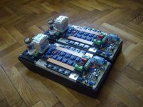
Several power stage was tested these has so far the best sound.
He also tested these with two pair power transistors lower rail voltage to but the result was not as good.
The amp has some interesting protection, didn't found the circuit yet.
You can see it from the picture.
The driver stage power supply is something else to (a monster with tube rectifier) ..
Will post a picture from that to if not a problem.
Greetings.
Attachments
Member
Joined 2009
Paid Member
That's a significant piece of hardware you're showing, and very useful to hear some impressions about the OPS. I am still thinking in my own mind what OPS I will use for my hybrid. Keep posting your impressions.
Hi Gaborbela,
Looks very interesting!... with no GNF it will have more of a tubby sound I think.
The OPS:
It has some features I'm not familiar with. You have a triple with 3 pairs which feeds the speaker through an inductor - which is good because it keeps the impedance of the OPS high for the tube stage. But you have a 4th pair of output devices which feeds the speaker through a resistor - what is this for ? and you hint at a protection circuit ?
The Vbe multiplier has a bias string made from 68k resistors to each rail. Perhaps there is no need for anything different but I wonder if there is a benefit in using bootstraps instead. This would mean replacing each 68 k resistor with a pair of resistors and then connecting the midpoint of each pair to the output with a 100uF capacitor ?
Maybe the base stoppers on the output devices could be smaller than 22R, say 2R2 even ? - just a small tweak.
Looking good !
Gareth, they look like 4 output pairs in parallel to me, and the inductor and the resistor are both part of Zobel network. Right? 😕
- Status
- Not open for further replies.
- Home
- Amplifiers
- Solid State
- 80W Hybrid Audio Amplifier!