Reading this post, it seems that the use of the D44H11 was motivated by Walt Jung's use of this pass transistor for his original 1995 article... In other words, AKM did not seem to have benefited from the work done by Didden since the original article.
My bad, the D44H11 is used by the Super Regulator, not the AKM board.
Too much reading while waiting for my delayed flight back home...
0805 Resistors
Didden is recommending the use of 0805 resistors for an SMD version of the Super Regulator, instead of the 0603 that we were planning to use.
Didden is recommending the use of 0805 resistors for an SMD version of the Super Regulator, instead of the 0603 that we were planning to use.
This post related to an SMD version of the Super Regulator is interesting.
I am going through the entire thread (1,726 posts!) trying to learn as much as possible about this circuit.
Super interesting so far...
I just finished reading the whole thread. What a ride! Highly recommended, especially the first 1,000 posts or so. Now, I need to learn more about the SilentSwitcher. Not as an alternative for the DAC's regulator, but for other parts of the overall project.
Learning about the Linear Audio Silent Switcher
I have been trying to understand how the Linear Audio Silent Switcher works (Cf. high-resolution picture). As far as I can tell, it is pretty close to the OSVA AAPSU01. The two boards have the following components in common:
- LT3471 Boost/Inverter
- TPS7A47 Low Noise Positive LDO
- TPS7A33 Low Noise Negative LDO
Now for the differences. The AAPSU01 includes:
- LT8609A Low EMI Buck Converter
- LT1965 Low Noise Positive LDO
For its part, the Silent Switcher seems to include:
- TPS6306x Buck Boost Converter (I could be wrong on this one)
I really like what the Silent Switcher is doing: taking USB's 5V as input and producing both ±15V and 5V as output. That's pretty much what we need for the DAC board, in combination with the Jung/Didden Super Regulators.
But I am willing to bet that using a component like the LT8609A from Analog Devices' Silent Switcher line of product can help further reduce EMI. And in a rather amusing way, Linear Audio is calling the board "Silent Switcher", but does not use any "Silent Switcher" chip from Analog Devices.
I will spend more time familiarizing myself with the AAPSU01's schematic before outlining a list of parts that could work for our needs. In the meantime, any additional references would be much welcome.
Last edited:
So, using a switching regulator is going to cause a lot of consternation among those here who feel that switchers sound bad. I don't think this is necessarily true at all, though they have a bad reputation from old or cheap designs.
SMPS / power conversion is complex enough to be its own discipline unto itself, but there are a few things to note. Buck regulators tend to have the lowest conducted output ripple, because the inductor is on the output side. Layout is critical, and it is very easy to make a product that fails EMC testing if care is not taken.
On the Silent Switcher line, I am not sure there is a lot of reason for it to be lower EMI than any other buck regulator with an external inductor. Their EMI bullet point is accompanied by text talking about spread spectrum modulation. Spread spectrum modulation will help you pass EMC testing - but it doesn't necessarily lower emissions. Your absolute peak will still be the same, but it moves around a little. This helps you pass emissions testing because almost all standards mandate a quasi-peak detector mode, which essentially weights signals based on repetition rate. Peak values are almost always a few dB higher than quasi-peak. Softer switching is a way to get lower EMI, but it can cost efficiency, so a lot of ICs don't do it.
The safest approach is to use modules with internal shielded inductors and switches like the LT uModule line or the TI modules. It's harder to mess up this way, you aren't responsible for the compensation or the layout of the most critical nodes.
Edit - I did just see the LT8609A claims to have slower edges to lower EMI, so it might be a good choice.
Last edited:
So, using a switching regulator is going to cause a lot of consternation among those here who feel that switchers sound bad. I don't think this is necessarily true at all, though they have a bad reputation from old or cheap designs.
SMPS / power conversion is complex enough to be its own discipline unto itself, but there are a few things to note. Buck regulators tend to have the lowest conducted output ripple, because the inductor is on the output side. Layout is critical, and it is very easy to make a product that fails EMC testing if care is not taken.
On the Silent Switcher line, I am not sure there is a lot of reason for it to be lower EMI than any other buck regulator with an external inductor. Their EMI bullet point is accompanied by text talking about spread spectrum modulation. Spread spectrum modulation will help you pass EMC testing - but it doesn't necessarily lower emissions. Your absolute peak will still be the same, but it moves around a little. This helps you pass emissions testing because almost all standards mandate a quasi-peak detector mode, which essentially weights signals based on repetition rate. Peak values are almost always a few dB higher than quasi-peak. Softer switching is a way to get lower EMI, but it can cost efficiency, so a lot of ICs don't do it.
The safest approach is to use modules with internal shielded inductors and switches like the LT uModule line or the TI modules. It's harder to mess up this way, you aren't responsible for the compensation or the layout of the most critical nodes.
Chris,
Thanks a ton for that.
To be clear, I was planning to use this circuit for the ±15V that is needed by the OpAmps and for the input of the NJM78, which themselves will be replaced by something better. But I was still planning to use the Jung Didden Super Regulator circuit for VREF.
And if anyone has any issue with switching regulators, they should have that discussion with experts like Didden, not me. As far as I can tell, Didden who has been designing really nice regulators for more than 30 years got pretty excited about the latest developments with switching regulators 3 or 4 years ago. In other words, if they're good enough for him, they're probably good enough for me, at least for a while. And I expect switching regulators to progress faster than my analog design skills unfortunately...
Regarding the μModule, I was looking at them, and I really liked what I saw. I agree with you that using them would dramatically reduce the risk of a bad layout and would certainly help with certification. I just could not find any examples of audiophile applications using them. Do you know of any?
My comment regarding EMI reduction was motivated by the video on this page. Of course, it's heavy on the marketing side, but it still seems to make sense.
One thing that wasn't clear to me is how to get clean 5V out of dirty 5V. Do you use a Boost/Inverter to get it to something like 6V then a low-noise positive LDO to get it back to 5V? Or is there a better way of approaching this?
Last edited:
Chris,
Thanks a ton for that.
To be clear, I was planning to use this circuit for the ±15V that are needed by the OpAmps and for the input of the NJM78, which themselves will be replaced by something better. But I was still planning to use the Jung Didden Super Regulator circuit for VREF.
And if anyone has an issue with switching regulators, they should have that discussion with experts like Didden, not me. As far as I can tell, Didden who has been designing really nice regulators for more than 30 years got pretty excited about the latest developments with switching regulators 3 or 4 years ago. In other words, if they're good enough for him, they're probably good enough for me, for a while...
Regarding the μModule, I was looking at them, and I really liked what I saw. I agree with you that using them would dramatically reduce the risk of a bad layout and would certainly help with certification. I just could not find any examples of audiophile applications using them. Do you know of any?
My comment regarding EMI reduction was motivated by the video on this page. Of course, it's heavy on the marketing side, but it still seems to make sense.
One thing that wasn't clear to me is how to get clean 5V out of dirty 5V. Do you use a Boost/Inverter to get it to something like 6V then a low-noise positive LDO to get it back to 5V?
I would still post-regulate any switcher with a linear regulator if you are able. As far as going 5V to 5V, yes you could boost and then regulate it back down. Ferrites and passive filtering are important here because most linear regulators don’t have the bandwidth to reject harmonics of the switching frequency. Even LT3045 really only works well out to 1 MHz or so.
I would still post-regulate any switcher with a linear regulator if you are able. As far as going 5V to 5V, yes you could boost and then regulate it back down. Ferrites and passive filtering are important here because most linear regulators don’t have the bandwidth to reject harmonics of the switching frequency. Even LT3045 really only works well out to 1 MHz or so.
Both were very much parts of the plan, but I'm really glad that you're confirming it.
This design would allow the DAC brick to be standalone and powered by regular USB, not just USB-C, which would be really nice...
So, using a switching regulator is going to cause a lot of consternation among those here who feel that switchers sound bad. I don't think this is necessarily true at all, though they have a bad reputation from old or cheap designs.
And for the past 8 years, Benchmark has been putting switching power supplies in all their new products...
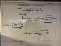
Power Supply Architecture
Here is a first shot at what our power supply architecture could be. It is optimized for the DAC brick, but it is designed to work for any brick of the OTO™ system. Furthermore, it is designed to support operations while connected to the mains or to a portable battery, both via the intermediation of a USB port.
The architecture is split into two main sub-components (see attached synoptic):
1. The Plate PSU Board located in the 4.5" × 4.5" plate.
2. The DAC PSU Board located in the 3" × 1.5" DAC brick.
The components susceptible of generating the most EMI are carefully located on the Plate PSU Board, so that they can be best shielded away from the sensitive components that are located in the DAC brick. And the connection between the plate and the brick is done thought the OTOBUS™.
With these requirements in mind, the OTOBUS™ interface was modified in order to provide the following power circuits:
+16 V
-16 V
+6 V
+3.3 V
These levels were chosen for the following reasons:
1. The DAC brick needs relatively clean ±15 V supplies for MVREF and MVDD, which need to be produced with a little bit of headroom, therefore ±16 V was deemed appropriate.
2. Many bricks (not just the DAC brick) will need very clean 5 V that can be produced by an ultralow noise linear regulator like the ADM7150 (thank you Chris!), but this component has a 0.6 V dropout at VOUT = 5 V, therefore 5.5 V would not provide enough headroom. 6 V was deemed sufficient, while ensuring a relatively low power dissipation.
3. Many bricks will be perfectly happy with a not-so-clean 3.3 V power supply. Therefore, directly providing it through the OTOBUS™ means that we won't have to add an extra regulator on these bricks.
4. We ran out of pins on the 40-circuit OTOBUS™, and cannot provide more power circuits without making some sacrifices in relation to some interfaces that are really important for our intended applications.
Plate PSU Board
It all starts with the 5 V power supply provided by the USB bus. There, our main idea was to use the LT3471 Boost/Interter. Obviously, we owe this design to Frex and his ultra-cool AAPSU01. This will give us the ±16 V levels that will feed the rest of the circuit.
Right there, we might have a problem though, because the +16 V level will be used for many things, while the -16 V level will be used only for producing a clean -15 V supply. Therefore, the imbalance might lead to some issues that we might want to prevent by using another step-up converter upstream of the LT3471 that would take +5 V up to something like 18 V, then feed this supply out to both the LT3471 and the LT8609A step-down converter — should we do that?
This LT8609A high efficiency, high speed synchronous monolithic step-down switching regulator will be used to get from +16 V or +18 V down to +6 V. This supply will be fed directly to the OTOBUS™, but also diverted to an ADM7150 ultralow noise,
high PSRR, RF linear regulator. This last major component of the board will be used to produce a very clean +3.3 V supply fed to the OTOBUS™. Of course, this might be a bit overkill, because we're not planning to re-regulate this supply on most bricks, therefore it won't remain that clean after having gone through the ERF8/ERM8 connectors of the OTOBUS™, but we should still try to make it as good as it can be from the source.
DAC PSU Board
The DAC PSU board won't make use of this +3.3 V VCC supply, but it will take the +6 V supply and feed it to a set of ADM7150 regulators that will produce very clean VDD supplies, as a replacement for the NJM78s used on the AKM evaluation board. Once again, this is probably overkill, but better safe than sorry. And using the same component on both PSU boards will allow us to leverage our R&D investments — designing a proper PCB layout for these regulators is not easy. Fortunately, the technical documentations coming out of Analog Devices and Linear are positively first class (Linear especially even more so than AD).
In addition, we will take the ±16 V supplies and feed them to a pair of TPS7A47/TPS7A33 that will give us very clean ±15 V supplies. Here, credit goes to Frex and Jan Didden with his Silent Switcher. These ±15 V supplies will give us MVDD directly, but will also be fed to a set of Jung/Didden super regulators adapted from this design. They will replace the circuits used on the AKM reference board, which use the obsolete SB1188 and the AD817 (no problem with that one). Instead, we will use the much better MJD44H11/MJD45H11 pass transistors and the AD825, which has proven so effective for the Jung/Didden Super Regulator, and generates 13dB less harmonic distortion at 1MHz than the AD817 (-76dB vs. -63dB). And that will give us the all-important VREFs.
Obviously, this is quite a complex circuit, with two separate boards, 5 or 6 different kinds of regulators, and 3 or 4 stages of regulation between USB and VREF. Nevertheless, if we want the best possible sound quality in the smallest amount of space available, this is probably the kind of thing that has to be done.
Clearly, I'm way over my head with this kind of design, so I must have made a lot of very stupid mistakes that I would love to be pointed out. Also, all this needs to be prototyped, tested, measured, and listened to before we can call it a valid design. But before we do any of that, I would love to get some high-level validation of whether any of this could work at all, because it will help me prioritize what has to be done next.
Cheers!
Note: We are currently looking at the LTM8049 µModule as an alternative to the LT3471, and we might use µModules as alternatives to other regulators currently selected, in order to simplify our design and increase our chances of getting something properly certified.
PS: Many thanks to Mark and Chris for their early coaching on regulators. I know that I had a very slow start there, so it might have been quite frustrating back in the middle of July... 😉
Attachments
Last edited:
Probably not a great idea to send the dac chip 3.3v from a remote regulator. Just send over +7v or +8v (because even 3.3v LDO linear regulators often regulate better with a little more input voltage, IME) and use local regulators to produce +5v or +3.3v where needed. Otherwise you may have all sorts of little interactions between different subsystems via power supply coupling, at least its a risk. You would need to test to see if it makes a difference in your application and with your PCB design. Allo Katnta and Benchmark DAC-3 each use several linear regulators. The DC/DC converters in Katana don't sound as good as external linear supplies no matter what Allo tried, including LT3042 post regulators.
Also, NJM7805 may turn out to sound a lot better for use with analog audio loads than ADM7150 does.
Lastly, I have two silent switchers here and a few 3.3v ADM7150 moudules. Don't use the silent switchers much, there was ground conducted noise passing through them from the wall wart they plugged into. If the switchers were run off a clean, e.g. linear, 5v source, then they might be usable for something in a dac.
A little more regarding ADM7150, they are good for digital loads IME, but never got them to sound as good as opamp buffers for AVCC use.
Enjoy the Kool-Aid though. All part of gaining experience. 🙂
Last edited:
Probably not a great idea to send the dac chip 3.3v from a remote regulator. Just send over +7v or +8v (because even 3.3v LDO linear regulators often regulate better with a little more input voltage, IME) and use local regulators to produce +5v or +3.3v where needed. Otherwise you may have all sorts of little interactions between different subsystems via power supply coupling, at least its a risk. You would need to test to see if it makes a difference in your application and with your PCB design. Allo Katnta and Benchmark DAC-3 each use several linear regulators. The DC/DC converters in Katana don't sound as good as external linear supplies no matter what Allo tried, including LT3042 post regulators.
Also, NJM7805 may turn out to sound a lot better for use with analog audio loads than ADM7150 does.
Lastly, I have two silent switchers here and a few 3.3v ADM7150 moudules. Don't use the silent switchers much, there was ground conducted noise passing through them from the wall wart they plugged into. If the switchers were run off a clean, e.g. linear, 5v source, then they might be usable for something in a dac.
A little more regarding ADM7150, they are good for digital loads IME, but never got them to sound as good as opamp buffers for AVCC use.
Enjoy the Kool-Aid though. All part of gaining experience. 🙂
Thanks for the feedback. To be clear: I am not using the 3.3 V supply in the DAC brick (look at the synoptic at the top, it's clearly marked as such). This supply will be used for other bricks that have non-critical components like rotary encoders. I hope you won't talk me into improving the power supply for rotary encoders to make them sound better... 😉
I also talked with a good friend, and he advised to do the following:
- Increase the differential between the two boards by going from ±16 V to ±20 V.
- Use the LT3471 of the Plate PSU Board only for the audio supply.
- Use another step-up converter on the Plate PSU Board to get the +6 V supply.
- Replace the TPS7A47 and TPS7A33 by linear regulators from Linear.
- Avoid low dropout regulators whenever possible.
I'll update the design accordingly.
- Use the LT3471 of the Plate PSU Board only for the audio supply.
- Avoid low dropout regulators whenever possible.
* LDO's can be good or perhaps essential for cleaning up the output of switchers.
* LDO's are probably preferred for the digital components of dacs.
* It takes very careful design of a switcher and post regulators to make it perform well enough for the analog part of high end audio. Enough time, effort, money should be able to do it though.
Interesting... There seems to be disagreement among the experts here. But to be perfectly honest, what you are writing makes a lot more sense to me, because LDOs have so much less noise than "high drop-out" regulators, that I have a hard time understanding why one should not use them for this application.
Thanks!
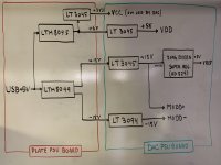
Updated Power Supply Architecture
Here is an updated power supply architecture based on the feedback I've received so far.
- The ±16 V circuits were replaced by ±18 V.
- The LT3471 was replaced by a μModule LTM8049.
- The LTM8049 was dedicated to the analog section.
- The LTM8049 was paired with an LTM8045 for the digital section.
- The TPS7A47/TPS7A33 were replaced by LT3045 and LT3094 LDOs.
- The ADM7150s were replaced by the same LT3045 LDO.
The LT3045 and LT3094 were selected because they're a good match for the +15 V and -15 V supplies. They both have an ultra low 800nV of RMS noise, 500mA of output current, and similar dropout voltages (235mV and 260mV respectively).
The LT3045 and LT3094 could be replaced by 200mA equivalent regulators (LT3042 and LT3093) if we find out that we do not need 500mA for some supplies.
The LT3045 regulators used for VCC 3.3 V and VDD 5 V could probably be replaced by simpler and cheaper LDO regulators, but I do not want to take any chances that this point. We can always streamline the design later on.
The +6 V circuit on the OTOBUS™ was kept at that level instead of bumping it to +7 V or +8 V because we're now using LDO regulators, therefore we probably do not need a higher differential. That being said, it should be very easy to change that voltage by adjusting some resistance values. Nevertheless, we went from ±16 V up to ±18 V in order to get ±3V of differential on the analog section, because we want the ability to play with different kinds of regulators there, and some might need a larger differential than the ±1V that ±16V circuits would give us for the ±15V that needs to be produced in the end for MVDD and MVREF.
Thoughts?
Attachments

Last edited:
...LDOs have so much less noise than "high drop-out" regulators, that I have a hard time understanding why one should not use them for this application.
Its because noise isn't everything, its just one factor. Making analog audio circuits sound good with LDOs is harder, particularly those circuits with low or zero PSRR.
Its because noise isn't everything, its just one factor. Making analog audio circuits sound good with LDOs is harder, particularly those circuits with low or zero PSRR.
Do you really mean low PSRR or high PSRR? Because the LT3045 and LT3094 are being marketed as "Ultrahigh PSRR" (76dB and 74dB at 1MHz respectively). Is that "ultrahigh" for an LDO but low in comparison to a non-LDO regulator? As a point of comparison, the LT3088 (a non-LDO regulator with a seemingly good reputation) has a PSRR of 20dB at 1MHz. So, what am I missing? I am reading these the wrong way?
Here is another example: the NCV8160, NCV8181, and NCV8163 from ON Semiconductor are being marketed as ultra-high PSRR by Mouser, and they offer 48dB, 48dB, and 60dB at 100KHz, so the numbers are likely to be much worse at 1MHz. That's a long way from 74dB... Or the TPS7A8101 , which only offers 54dB at 1MHz. And I could go on and on.
Unless I missed something, these LT3045 and LT3094 are pretty darn impressive.
Last edited:
Do you really mean low PSRR or high PSRR?
Low PSRR of the analog load, not the regulator.
Those regulators are impressive given the way the way they are measured as shown in the data sheets. That doesn't mean they measure them in some way to see how good they sound with low or zero PSRR loads, such as for switched resistor dac output bias. Its up to designers to devise their own tests if they have special needs.
Last edited:
Low PSRR of the analog load, not the regulator.
Those regulators are impressive given the way the way they are measured as shown in the data sheets. That doesn't mean they measure them in some way to see how good they sound with low or zero PSRR loads, such as for switched resistor dac output bias. Its up to designers to devise their own tests if they have special needs.
Okay, but you're talking about VREF then, which will be fed by the Jung/Didden Super Regulator, not by the LT3045/LT3094 LDOs directly. So, how would the DAC output bias be affected by the LDOs with respect to PSRR?
Adding the synoptic again for references purposes.
Attachments
Last edited:
- Home
- Source & Line
- Digital Line Level
- 8 × AK5578EN + 8 × AK4499EQ ADC/DAC Boards