DAC Brick Stack
I am now working on the DAC brick, and while everything will need to be tested against our reference system, I am trying to figure out the best way to stack the different boards that will go into that brick. Most likely, we will have four PCBs:
- PCB 1 Bottom: Clock oscillators
- PCB 1 Top: Linear regulators and digital isolators
- PCB 2 Bottom: Jung/Didden regulators, resistors, and small capacitors
- PCB 2 Top: DAC and large capacitors
- PCB 3 Bottom: Operational amplifiers
- PCB 3 Top: Mini XLR connector
- PCB 4: Top cover
The thinking goes like this:
PCB 1 Bottom: Digital oscillators
We want the two NZ2520SDA clock oscillators to be as far away from the DAC chip as possible. Therefore, with this arrangement, we have two PCBs that separate them. Also, it should be noted that the STM32H743 MCU is not part of that stack, because it will be mounted on the underlying plate, driving three individual bricks. Here, we're looking at the stack of boards that will fit within a single brick. This board will connect to the underlying plate through a pair of Samtec 40-circuit ERM8 connectors used for the OTOBUS™, with a 7mm mating height (the clock oscillators have a very low profile). For this side of the board, my only question is this: can we put anything else that would not be affected by the oscillators too much, like the large capacitors that are used for the linear regulators, or some of the linear regulators themselves?
PCB 1 Top: Linear regulators and digital isolators
There, we will have at least 8 linear regulators, and possibly more, depending on how we decide to go from 15V down to 5V. This is important, because we probably cannot use the 5V supply directly provided by the OTOBUS™. This supply will be sufficient for non-critical controls such as rotary encoders, but for a DAC circuit, we need very clean power supplies. Therefore, we will have to make our 5V on board, unless we decide to add a 6V or 5.5V power supply circuit to the OTOBUS™ (I am seriously considering this option, but we're out of pins already). This side of the board will also include the Silicon Labs CMOS digital isolators that will bring clean digital signals to the DAC board.
PCB 2 Bottom: Jung/Didden regulators, resistors, and small capacitors
This side of the second board will have as many capacitors and resistors as possible, plus the Jung/Didden regulators. Because these components have a fairly low profile, we might be able to use the Mill-Max Super Low-Profile Sockets that have a 3.94mm mating height, especially if we position the components on this side of the board and the top side of the lower board in such a way that they do not interfere with each other. This will be a tricky exercise, but if it works out, we'll be able to save 2.66mm of total height for the brick.
PCB 2 Top: DAC and large capacitors
This side of the second board will have the brick's most important component: the AK4499EQ DAC. But it will also be host for the 4 large 470μF capacitors that need to be mounted really close to the DAC. After discussions with the Oracle and Wizard of Auburn (they'll recognize themselves), I am tempted to drop the tantalum capacitors and go for the Panasonic OS-CON conductive polymer aluminum solid capacitors. Unfortunately, these capacitors are quite large, therefore we'll have to be clever about how to make them fit...
PCB 3 Bottom: Operational amplifiers
This side of the third and last board will have the four OPA1612 operational amplifiers. Here, we're assuming that mounting them on a separate board away from the DAC chip won't create too many problems. What makes us think that way is that the linear distance should actually be the same as the one found on the AKM evaluation board, and we will use high-quality machined pin sockets and headers for connecting the two boards together. Also, by doing so, we get the operational amplifiers mounted on the same board as the mini XLR connector.
PCB 3 Top: Mini XLR connector
Finally, the top of the third board will be host for the mini XLR connector. Here, the idea is that the board will actually be smaller than the other ones. Boards 1 and 2 will be 35mm × 35mm, but board 3 will be only 35mm × 15mm, allowing the four large capacitors mounted on the top of board 2 to stand next to the bottom of the mini XLR connector. And this arrangement is the reason why we have to use a mini XLR connector. Of course, these are less reliable than standard XLR connectors, but the draconian dimensioning constraints that we gave ourselves do not give us very many other options. That being said, these connectors are good enough for the $9,000 Scorpio portable mixer-recorder, therefore they should be good enough for us. The only consequence of such a design is that we will only have a single mono output (using a 3-pole connector) or two mono outputs (using a 5-pole connector), thereby losing the four mono outputs option. That being said, we could recover the latter by making the brick taller, but I would like to avoid that if at all possible.
PCB 4: Top cover
This PCB will only be used to mount the Mini XLR connector, unless we find a way to add bargraphs to it (this would be totally awesome).
So, how tall would the brick be? Well, let's do the math:
- Plate to board 1 mating: 7mm
- Board 1 thickness: 1.6mm
- Board 1 to board 2 mating: 3.96mm
- Board 2 thickness: 1.6mm
- Board 2 to board 3 mating: 3.96mm
- Mini XLR connector up to top of cover board: 9.17mm
Total: 27.3mm
For a 38mm × 38mm brick, that would still make it a fairly low-profile one, and knowing that our standard bricks will be 20mm tall, we might want to relax our height constraints a bit and make the brick 30mm tall.
So, before I do any more work on this, what part of that design is totally flawed?
Last edited:
Why do you want the oscillators far away? I'd normally think the opposite.
Far away is probably not the best term indeed. What I meant is that you want them isolated from the DAC chip, therefore "far away" from a layering standpoint (two PCBs in between them). But from the standpoint of trace length, you indeed want them as close to each other as possible (in our case, about 3/4").
Really sorry for the confusion.
Last edited:
Far away is probably not the best term indeed. What I meant is that you want them isolated from the DAC chip, therefore "far away" from a layering standpoint (two PCBs in between them). But from the standpoint of trace length, you indeed want them as close to each other as possible (in our case, about 3/4").
Really sorry for the confusion.
I'm not sure. I haven't compared, but if you are running the clock through connectors or even just vias you introduce impedance discontinuities. I see a lot of high end converter reference designs that place the clock right next to the converter IC, on the same layer.
I'm not sure. I haven't compared, but if you are running the clock through connectors or even just vias you introduce impedance discontinuities. I see a lot of high end converter reference designs that place the clock right next to the converter IC, on the same layer.
But don't you want to isolate the DAC from the EMI generated by the oscillators?
But don't you want to isolate the DAC from the EMI generated by the oscillators?
Maybe it would be helpful to take a look at how Allo designed the compact and somewhat modular Katana dac. There is a dac board which includes shielded clocks each with a dedicated voltage regulator (in fact most of the dac board does local voltage regulation and filtering), then there are some connectors which go down to the RPi board where files are stored, and connectors going up from the dac board to the output stage board. Some more connectors attach the output stage board to the next board up in the stack which is the MCU control, incoming power supply, and power conditioner board. That type of organization into modular form makes good sense from an EE perspective. I know for a fact they studied Ott carefully and still do. The lead engineer on the project says he has read Ott three times from cover to cover, and keeps a copy of The Art of Electronics next to his bed. Not a bad idea to help learn how this stuff works. 🙂
Last edited:
But don't you want to isolate the DAC from the EMI generated by the oscillators?
Not by creating an antenna that radiates EMI...
Problem with C6, C14, C35, C90 Capacitors
I am currently working on re-creating a schematic for the AKD4499-B0-00E evaluation board, and I believe that the schematic provided on page 58 of the manual is incorrect. The C6, C14, C35, C90 capacitors that are located close to the AK4499EQ and marked 220µF seem to be 470µF on the actual evaluation board. And if they're not, I do not know where these 220µF capacitors are on the board, and where the actual 470µF capacitors are supposed to be found on the schematic. Therefore, I will assume that the datasheet is incorrect and that 470µF capacitors should be used instead.
As far as I can tell, the board is using four EKMQ500EMC471MJ20S capacitors, or something very similar. The closest equivalent I could find in SMD format is the 20SVPK470M. The main differences are these (reference board first):
- Voltage Rating: 50 VDC vs. 20 VDC (should be acceptable)
- Ripple Current: 540 mA vs. 1.56 A (better)
- Maximum Operating Temperature: 105 °C vs. 125 °C (better)
The main benefit of the 20SVPK470M is that its width is 8.3mm, which means that it should fit perfectly at the top of the DAC board (board #2), really close to the DAC chip. And its height is only 11.9mm, with a diameter of 8mm.
With such a height, we will have to mount the XLR board (board #3) in such a way that these four capacitors rise above the board, but we could keep the board with a 35mm × 35mm footprint by cutting four 9mm diameter round holes in it. That way, the top of the capacitors would go through the board, but it would still allow us to mount quite a few components around them. It's a bit funky, but I do not see any reason why we could not do that.
Last edited:
...I do not know where these 220µF capacitors are on the board, and where the actual 470µF capacitors are supposed to be found on the schematic...
You probably should carefully pry up and remove the dac daughterboard from the motherboard. You will find some additional components down there that you will need to account for.
It is strongly recommended to note the orientation of the daughterboard before removal so as not to inadvertently reinstall it in a rotated position. Taking a picture first may be a good idea.
Not by creating an antenna that radiates EMI...
I will try to avoid that indeed. Thank you.
Maybe it would be helpful to take a look at how Allo designed the compact and somewhat modular Katana dac. There is a dac board which includes shielded clocks each with a dedicated voltage regulator (in fact most of the dac board does local voltage regulation and filtering), then there are some connectors which go down to the RPi board where files are stored, and connectors going up from the dac board to the output stage board. Some more connectors attach the output stage board to the next board up in the stack which is the MCU control, incoming power supply, and power conditioner board. That type of organization into modular form makes good sense from an EE perspective. I know for a fact they studied Ott carefully and still do. The lead engineer on the project says he has read Ott three times from cover to cover, and keeps a copy of The Art of Electronics next to his bed. Not a bad idea to help learn how this stuff works. 🙂
Both books are in the mail!
Do you know where I can find high-resolution pictures of all three boards on both sides?
Do you know where I can find high-resolution pictures of all three boards on both sides?
Sorry, no. It would be great if you could post them here if you are the first one to take the pictures.
You probably should carefully pry up and remove the dac daughterboard from the motherboard. You will find some additional components down there that you will need to account for.
It is strongly recommended to note the orientation of the daughterboard before removal so as not to inadvertently reinstall it in a rotated position. Taking a picture first may be a good idea.
Fair enough, but where are the four 470µF capacitors on the schematic? I sure cannot find them on page 58...
Sorry, no. It would be great if you could post them here if you are the first one to take the pictures.
I sure will!
...where are the four 470µF capacitors on the schematic? I sure cannot find them on page 58...
I don't see them there either. That may not be the only error on that page of the schematic. I noticed before that some of the silkscreen part numbers don't match up with the part numbers on the schematic, they seem to located on different channels of the dac chip. Of course, it is a rev 0 version of the eval board manual, so errors may be corrected by AKM eventually. Maybe good to print out that page and markup any errors you find for future reference.
Last edited:
I don't see them there either. That may not be the only error on that page of the schematic. I noticed before that some of the silkscreen part numbers don't match up with the part numbers on the schematic, they seem to located on different channels of the dac chip. Of course, it is a rev 0 version of the eval board manual, so errors may be corrected by AKM eventually. Maybe good to print out that page and markup any errors you find for future reference.
And I am willing to bet that the four large capacitors that are mounted underneath the board are also 470µF models... But I won't remove that board until I get it up and running, just in case I break it during removal. Call me chicken!
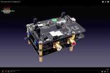
Katana Board Video
This video is a great introduction to the Allo Katana DAC. I took several screenshots that I will add to dedicated posts. A lot can be learned from this setup indeed. Thanks a lot to Mark for pointing us in this direction. It should be super helpful.
This video is a great introduction to the Allo Katana DAC. I took several screenshots that I will add to dedicated posts. A lot can be learned from this setup indeed. Thanks a lot to Mark for pointing us in this direction. It should be super helpful.
Attachments
Katana DAC Board
This is the Katana DAC board (top and bottom), which is the lowest board on the Katana stack shown on the previous post. The ESS DAC is on the left and the NDK clock oscillator is on the right, both with its own shield. Conclusion: we should mount the clock oscillators on the same board as the DAC chip, and we should shield both. The clock oscillator should have no problem fitting between two 470µF capacitors.
This is the Katana DAC board (top and bottom), which is the lowest board on the Katana stack shown on the previous post. The ESS DAC is on the left and the NDK clock oscillator is on the right, both with its own shield. Conclusion: we should mount the clock oscillators on the same board as the DAC chip, and we should shield both. The clock oscillator should have no problem fitting between two 470µF capacitors.
Attachments
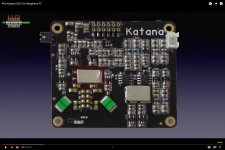

...The clock oscillator should have no problem fitting between two 470µF capacitors.
Well, except perhaps that it first needs to be decided how the USB board will be clocked. Clocks are often located on it and used to help with re-clocking signals post-galvanic isolation. Or, clocks may be located externally from the USB board and the board configured to signal which of the two external clocks is needed to be enabled at any particular time.
This area is one where Katana differs from many dacs. Katana uses an ESS dac chip operating in master I2S mode, whereas AKM dacs don't support acting as I2S master.
- Home
- Source & Line
- Digital Line Level
- 8 × AK5578EN + 8 × AK4499EQ ADC/DAC Boards