The datasheet is not very good.
I don't know if you can also add 3D Bodies in Circuit Studio but try to get the STEP file of this part either at the website of Nexperia or at 3D ContentCentral - Free 3D CAD Models, 2D Drawings, and Supplier Catalogs.
You can use it in the 3D view to check your footprint.
When creating a pad you have the copper area (aka solder land in the datasheet), solder paste( I think thats easy what it is) and the solder mask opening which is the area between the copper area and the solder mask.
The footprint example in the datasheet suggests to have no solder mask isolation between the pads. It can work but in my opinion it is much more secure to have solder mask between pads to avoid the risk of a short. Solder mask should at least be 0,1mm wide that's what manufacturers I know of are able to produce and it also works with most footprints.
The datasheet says that the pads are 0.27mm wide max. You can use 0.3mm wide pads to be on the safe side and use a solder mask expansion of 0.05mm. For these values your solder mask between two pads will be 0.1mm wide.
Last edited:
The datasheet is not very good.
I don't know if you can also add 3D Bodies in Circuit Studio but try to get the STEP file of this part either at the website of Nexperia or at 3D ContentCentral - Free 3D CAD Models, 2D Drawings, and Supplier Catalogs.
You can use it in the 3D view to check your footprint.
When creating a pad you have the copper area (aka solder land in the datasheet), solder paste( I think thats easy what it is) and the solder mask opening which is the area between the copper area and the solder mask.
The footprint example in the datasheet suggests to have no solder mask isolation between the pads. It can work but in my opinion it is much more secure to have solder mask between pads to avoid the risk of a short. Solder mask should at least be 0,1mm wide that's what manufacturers I know of are able to produce and it also works with most footprints.
The datasheet says that the pads are 0.27mm wide max. You can use 0.3mm wide pads to be on the safe side and use a solder mask expansion of 0.05mm. For these values your solder mask between two pads will be 0.1mm wide.
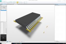
Yes, CircuitStudio supports 3D bodies. Here is an example for a STEP file that seems to be working fine. But the one I got from 3Dcontentcentral.com for the SOT765-1 seems to be off. As far as I can tell, it's a bit of an hit-or-miss game, and I might be better off designing my own 3D bodies...
I think I now understand what solder paste and solder land mean in the NXP terminology, but I am still at a loss on how to implement them in Altium. Here is another datasheet that is slightly less confusing. On page 3/5, we have a large SLx × SLy exposed die pad and 24 SPx × SPy solder paste pads. I am assuming that the solder paste pads must be designed using the "Top Paste" layer, but what about the exposed die pad, which is just copper? Should it be "Top Layer"? Does "Top Layer" mean copper pad? If so, whenever I select "Top Layer" in CircuitStudio, I get a "Top Paste" and "Top Solder" added as well, but in this case I do not want any paste. Am I missing something, because the paste needs to be broken down into 24 Top Paste pads. So, my question is this: how do I create a copper-only pad without any paste?
Attachments
Last edited:
Just. Give. Up.
I think you're misunderstanding what it is I'm trying to do here.
I am not trying to say I am right, first and foremost I am trying to get you to understand what it is I am trying to say. Which, up until now, you don't seem to have grasped.
The LRCK is not a critical clock and does not drive data conversion in these DACs. MCLK or divided MCLK does which is why it is required to be synchronous with the other I2S clocks.
Okay then please explain why ESS say that removing jitter on the data clocks/lines is important and that one of the main points of their ASRC is to do just this.
Can you explain that? Can you?
Yes, CircuitStudio supports 3D bodies. Here is an example for a STEP file that seems to be working fine. But the one I got from 3Dcontentcentral.com for the SOT765-1 seems to be off. As far as I can tell, it's a bit of an hit-or-miss game, and I might be better off designing my own 3D bodies...
I think I now understand what solder paste and solder land mean in the NXP terminology, but I am still at a loss on how to implement them in Altium. Here is another datasheet that is slightly less confusing. On page 3/5, we have a large SLx × SLy exposed die pad and 24 SPx × SPy solder paste pads. I am assuming that the solder paste pads must be designed using the "Top Paste" layer, but what about the exposed die pad, which is just copper? Should it be "Top Layer"? Does "Top Layer" mean copper pad? If so, whenever I select "Top Layer" in CircuitStudio, I get a "Top Paste" and "Top Solder" added as well, but in this case I do not want any paste. Am I missing something, because the paste needs to be broken down into 24 Top Paste pads. So, my question is this: how do I create a copper-only pad without any paste?
I am not sure about CircuitStudio, but here is how it works in Altium Designer.
For the top and bottom layers, you get the following:
1. Top Layer / Bottom Layer (copper layers, positive)
2. Top Overlay / Bottom Overlay (silkscreen, positive)
3. Top Solder / Bottom Solder (soldermask, negative)
4. Top Paste / Bottom Paste (solder paste, positive)
So, your pads are on the copper layers and Altium by default will create soldermask openings and solder paste fills where your pads are +/- some distance specified by the design rules of the current PCB. The rules that control that are called Solder Mask Expansion and Paste Mask Expansion. They should be set to whatever values your fabricator can guarantee. I would only change it manually on pads where you need to deviate for specific reasons.
Is there a reason you don't want paste on your pads? That's pretty much what you want in all cases. If you're assembling by hand then you just ignore that file. In any case, if you need to modify the paste for a specific reason you can select the Top Paste layer (in the PCB library editor in the footprint, or on the PCB directly if you don't want to modify the footprint) and delete or change the shapes on it.
Not sure about CircuitStudio, but Shift+S in AD will toggle layer selection mode and let you display only the layer you have selected at the bottom. This can help in visualizing / selecting objects.
Last edited:
I think you're misunderstanding what it is I'm trying to do here.
I am not trying to say I am right, first and foremost I am trying to get you to understand what it is I am trying to say. Which, up until now, you don't seem to have grasped.
Okay then please explain why ESS say that removing jitter on the data clocks/lines is important and that one of the main points of their ASRC is to do just this.
Can you explain that? Can you?
I grasped it. Please go create a separate thread for this if you want to continue your discussion. I will not post again on this topic in this thread.
I don't care what ESS says in some random PDF. If they say that, you're probably misinterpreting it, as you've misunderstood everything else going on here. Your appeal to some random PDF as authority against fact is not convincing and it's not logically sound.
I am not sure about CircuitStudio, but here is how it works in Altium Designer.
For the top and bottom layers, you get the following:
1. Top Layer / Bottom Layer (copper layers, positive)
2. Top Overlay / Bottom Overlay (silkscreen, positive)
3. Top Solder / Bottom Solder (soldermask, negative)
4. Top Paste / Bottom Paste (solder paste, positive)
So, your pads are on the copper layers and Altium by default will create soldermask openings and solder paste fills where your pads are +/- some distance specified by the design rules of the current PCB. The rules that control that are called Solder Mask Expansion and Paste Mask Expansion. They should be set to whatever values your fabricator can guarantee. I would only change it manually on pads where you need to deviate for specific reasons.
Is there a reason you don't want paste on your pads? That's pretty much what you want in all cases. If you're assembling by hand then you just ignore that file. In any case, if you need to modify the paste for a specific reason you can select the Top Paste layer (in the PCB library editor in the footprint, or on the PCB directly if you don't want to modify the footprint) and delete or change the shapes on it.
I think I understand what you wrote, and I agree with it.
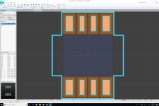
The reason why I don't want paste on pads is for this package, for which we don't want paste on the entire exposed die. Instead, we want 24 smaller paste areas. Does that make sense?
And as far as I can tell, CircuitStudio works exactly like Designer for all these basic things. This page provides a highly detailed comparison between the two versions.
Last edited:
I think I understand what you wrote, and I agree with it.
The reason why I don't want paste on pads is for this package, for which we don't want paste on the entire exposed die. Instead, we want 24 smaller paste areas. Does that make sense?
Yep, I have seen that done like in the PDF.
For generic packages like SOTxxxx I usually just create them with the Altium IPC Compliant Footprint Wizard (not sure if that exists in CS). I have segmented the paste layer like the NXP PDF shows but often I don't. I usually throw a few vias in the pad and make sure the bottom is tented. Sometimes the paste segmentation is handled in processing by your assembly vendor anyway.
It seems like CS should behave the same, but the GUI looks a lot different outside of the editor windows.
Last edited:
Yep, I have seen that done like in the PDF.
For generic packages like SOTxxxx I usually just create them with the Altium IPC Compliant Footprint Wizard (not sure if that exists in CS). I have segmented the paste layer like the NXP PDF shows but often I don't. I usually throw a few vias in the pad and make sure the bottom is tented. Sometimes the paste segmentation is handled in processing by your assembly vendor anyway.
It seems like CS should behave the same, but the GUI looks a lot different outside of the editor windows.
That explains! No, CS does not include the IPC footprint wizard.
Yes, the UI looks a bit different, mostly because CS uses ribbons while Designer menus.
Thanks a lot Chris, this is going to save me a lot of time and frustration. Much appreciated.
That explains! No, CS does not include the IPC footprint wizard.
Yes, the UI looks a bit different, mostly because CS uses ribbons while Designer menus.
Thanks a lot Chris, this is going to save me a lot of time and frustration. Much appreciated.
And I think I found a way to make it work for the SOT765-1: a negative value (-0.05mm) for the Paste Mask Expansion and 0mm for the Solder Mask Expansion.
And I think I found a way to make it work for the SOT765-1: a negative value (-0.05mm) for the Paste Mask Expansion and 0mm for the Solder Mask Expansion.
Just make sure before you have any boards made that you run Design Rule Check to make sure you don't have any violations.
I would make sure you really want 0mm Solder Mask Expansion. This means that any slight registration issues will result in solder mask on your pads.
Solder mask -
FEDEVEL Forum
Just make sure before you have any boards made that you run Design Rule Check to make sure you don't have any violations.
I would make sure you really want 0mm Solder Mask Expansion. This means that any slight registration issues will result in solder mask on your pads.
Solder mask -
FEDEVEL Forum
I think you're right. I just set it to "Expansion value from rules", and it still works, so I'll leave it at that.
Bottomline: all that was needed is a negative value for the Paste Mask Expansion. Well, that cost me a full day of work, but at least I'm starting to understand all these layers a bit more...
As I said before use 0.05mm or 0.07mm Solder Mask Expansion.
I don't recommend using the Solder Mask Expansion from rules option because of Parts with a small pitch need a smaller solder mask expansion to at least get the minimum solder mask width of 0.1mm between pads and for parts with a bigger pitch you should at least use a solder mask expansion value of 0.07mm.
A solder mask opening between the copper pad and the solder mask can also prevent solder paste from running over the solder mask and therefore prevent shorts between pins.
I absolutely don't recommend using a Solder Mask Expansion value of 0mm!
You can also add manual paste mask to a pad by entering a high value negative paste mask expansion and drawing the paste mask manually on the top paste layer.
For custom pad shapes you have to do it eitherway!
Last edited:
Agreed. It’s fine to use from rules, but you must have set them up properly.
I’m not even sure if CircuitStudio has component classes and other features you can use to scope rules with in queries.
I’m not even sure if CircuitStudio has component classes and other features you can use to scope rules with in queries.
Last edited:
BTW, does the AKD4499 eval board come with documentation?
I can't find any info online!
It does but you have to ask AKM for it for now for some reason. PM me and I can send it to you.
As I said before use 0.05mm or 0.07mm Solder Mask Expansion.
I don't recommend using the Solder Mask Expansion from rules option because of Parts with a small pitch need a smaller solder mask expansion to at least get the minimum solder mask width of 0.1mm between pads and for parts with a bigger pitch you should at least use a solder mask expansion value of 0.07mm.
A solder mask opening between the copper pad and the solder mask can also prevent solder paste from running over the solder mask and therefore prevent shorts between pins.
I absolutely don't recommend using a Solder Mask Expansion value of 0mm!
You can also add manual paste mask to a pad by entering a high value negative paste mask expansion and drawing the paste mask manually on the top paste layer.
For custom pad shapes you have to do it eitherway!
Understood! I will follow your advice.
Agreed. It’s fine to use from rules, but you must have set them up properly.
I’m not even sure if CircuitStudio has component classes and other features you can use to scope rules with in queries.
No, there is no support for object classes in CS unfortunately.
But none of these features would justify the price tag at this stage of the project.
Footprints
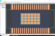
Following the different pieces of advice that I received from sciencesky and chris719, I have updated the footprints for SOT765-1 and SOT1331-1. setting proper values for the Paste Mask Expansions and Solder Mask Expansions. And by using a large value for the former on SOT1331-1, I managed to fully expose the die pad, then add the 24 segmented paste pads.
For both footprints, I also made sure to include the boundaries for the occupied areas on the "Courtyard Top" layer. For these, I set a width of 0.1mm, but I don't think it matters, since it won't be printed anywhere. Instead, it's just used as a way to make sure that components are not placed too close to each other on the PCB.
Many thanks to sciencesky and chris719 for their help! I've learned a lot in the process.
And I sure am glad to go through all this for a seemingly trivial project like an encoder with LED ring, because making mistakes for it will be a lot less painful than making mistakes for the AK4499EQ-powered DAC board.. Learning to walk before we run...
Attachments
Last edited:
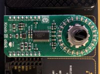
Board Close Up
For reference purposes, here is a high-resolution of the board we are re-creating in mikroBUS S-size.
For reference purposes, here is a high-resolution of the board we are re-creating in mikroBUS S-size.
Attachments
Last edited:
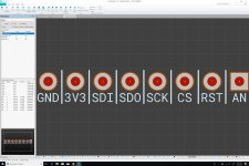
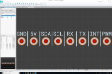
mikroBUS Footprints
Here are the footprints for the two mikroBUS connectors (Left and Right). Per specification, the holes have a 35 mils diameter, even though the datasheet for the 826647-8 component that I am planning to use recommends 1 mm. I suspect that the MikroE Click Board is using a different set of headers, but I do not have a complete BOM for it yet (I asked for it, but I'm not sure they'll be willing to share it).
The mikroBUS specification mandates all individual pin markings, but it's possible that we get rid of them on high-density boards. Also, the specification indicates that the add-on board's name must be printed at the bottom of the board. Unfortunately, this is where we are planning to have one of the two Hirose connectors for connecting the mezzanine board populated with our 24 LEDs to the base board. Therefore, we might put the board's name somewhere else, possibly on the mezzanine board itself, or on the backside of the base board.
And quite frankly, these markings are much less important than the pinouts, because our users won't really mess with individual pins. Instead, the individual brick itself will be their smallest unit of work.
Attachments
- Home
- Source & Line
- Digital Line Level
- 8 × AK5578EN + 8 × AK4499EQ ADC/DAC Boards