I would much rather do that indeed, because blind holes in PCBs seem to be on the exotic side, therefore super expensive. But finding an SMD connector without any indexing pin and a fairly tall mating height is not super easy, especially because the mating height is not a standard parameter on the distributors' websites. I'll keep looking though.
You might want to look at Samtec's options. Hard to tell from the site but the Razor Beam series might have an optional retention pin. Their board guides are usually designed with paste-in-hole reflow soldering in mind, so it could be an option with a blind hole depending on the specifics.
http://suddendocs.samtec.com/processing/pih-short-features-thick-pcb-final-edit.pdf
Very impressive product lineup!
And it seems that all these connectors come with indexing pins. Therefore, we'll have to find a way to either drill blind holes in the PCB or cover them somehow.
And it seems that all these connectors come with indexing pins. Therefore, we'll have to find a way to either drill blind holes in the PCB or cover them somehow.
As far as the placement outline is concerned, the Click Board is not using it for most of its components, and I'm not sure that we need it either, especially on such a small board. What's your take?
Starting to build your own parts library it is good to do it right from the beginning. A placement outline is a good thing to have so you know how close you can place parts together.
And remember smaller parts shouldn't be too close to taller parts because taller parts block airflow during the soldering process.
I see. Just to be clear: you make a difference between what you call "placement outline" that is on the overlay layer (the silkscreen for markings) and what the NXP datasheets call the "occupied area" that is on the courtyard layer. I am assuming that the former contains the latter, and that the former is used to incorporate a lot of the "fuzzy" rules like the one you mentioned in relation to airflow.
If so, that makes perfect sense, and I will add these placement outlines on all my components.
How thin do you draw this placement outline usually?
And yes indeed, I am starting to build my own library, and this is a ton of work (a lot more than I was expecting), and I'd rather get it right from the start.
Thanks a ton again for your help, this is fun.
I don’t think you really need to worry about the silkscreen outline too much (in my opinion). Altium will show you the bounding box as you select or move the part on the PCB editor. I normally see designs that are so small or dense that there is no room for silkscreen outlines. Design rules will flag any collisions or violations.
A placement outline is a good thing to have so you know how close you can place parts together.
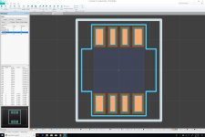
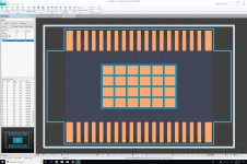
Here are the footprints with the placement outlines (0.1mm thick).
Attachments
I don’t think you really need to worry about the silkscreen outline too much (in my opinion). Altium will show you the bounding box as you select or move the part on the PCB editor. I normally see designs that are so small or dense that there is no room for silkscreen outlines. Design rules will flag any collisions or violations.
Too late... 😉
Ground on Mezzanine Board
I am currently in the process of designing the schematic for the base board of the E1 brick (single encoder with LED ring). As mentioned earlier, this brick is inspired from this Click Board, for which MikroE is kind enough to provide a schematic (but they declined to provide a BOM, as expected).
My first question is this: while the schematic document displays a standard copyright notice at the bottom (including an "All rights reserved." mentioned), I am assuming that it is acceptable for us to design our board according to this schematic. In this context, what would not be acceptable would be to make a "Xerox" copy of the original document and put our name on it for example. Does anyone have a different interpretation of intellectual property laws and best practices in the industry?
My second question is this: on the Click Board, the 24 LEDs are mounted directly on the board. The anodes are connected to VCC 3V3 and the cathodes are connected to the outputs pins of the LED driver. On our brick, we will have two separate boards: the base board with the LED driver, and a mezzanine board with the LEDs. As can be seen on the attached schematic (still very much a work in progress), we are using a 30-circuit connector between the base board and the mezzanine board, using the 30 pins in the following fashion:
- 24 × LED outputs
- 4 × VCC 3V3
- 2 × GND
From a schematic standpoint, the two GND circuits are not needed, since the LEDs only need VCC and driver outputs. Nevertheless, I am assuming that grounding the mezzanine board is a good idea. Please correct me if I am wrong. Also, I am assuming that VCC should use more circuits than GND (4 vs. 2), since VCC is actually used. I could have used 5 circuits for VCC and a single one for GND, but I liked the symmetry of the 4 + 2 combination. Please let me know if you would do things differently.
My last question is this: I have set a few document parameters like Title and Author, but they do not show up on the cartouche at the bottom right of the schematic sheet. Any idea why?
Attachments

Last edited:
My first question is this: while the schematic document displays a standard copyright notice at the bottom (including an "All rights reserved." mentioned), I am assuming that it is acceptable for us to design our board according to this schematic. In this context, what would not be acceptable would be to make a copy of the original document and to put our name on it for example. Does anyone have a different interpretation of intellectual property laws and best practices in the industry?
What follows is not legal advice (only a lawyer can give legal advice; and, I am not a lawyer):
I don't believe it is okay to change the name on a schematic and call it your own, any more than it would be okay to do that with a work of visual art. Copyright seems to be intended to protect a particular expression of an idea or ideas, not the underlying idea(s) themselves. Thus, copying a particular expression how how a circuit is interconnected would seem to be prohibited. Expressing your own depiction of circuit underlying interconnections might be another matter. Some have said, if some minor changes are made (from the perspective of an engineer) it can be enough to provide some legal protection. Probably take a lawyer to to tell you how much in the way of change would be advisable to stay reasonably safe.
That said, if no entity on your side has deep pockets then there may not be so much incentive to sue you.
Last edited:
What follows is not legal advice (only a lawyer can give legal advice; and, I am not a lawyer):
I don't believe it is okay to change the name on a schematic and call it your own, any more than it would be okay to do that with a work of visual art. Copyright seems to be intended to protect a particular expression of an idea or ideas, not the underlying idea(s) themselves. Thus, copying a particular expression how how a circuit is interconnected would seem to be prohibited. Expressing your own depiction of circuit underlying interconnections might be another matter. Some have said, if some minor changes are made (from the perspective of an engineer) it can be enough to provide some legal protection. Probably take a lawyer to to tell you how much in the way of change would be advisable to stay reasonably safe.
That said, if no entity on your side has deep pockets then there may not be so much incentive to sue you.
I think we're on the same page. Just to be clear: I wrote "what would not be acceptable" in relation to making a copy of the original document and putting our name on it. And my understanding is that what we are doing is sufficiently derivative to be acceptable. Furthermore, MikroE is in the business of selling development kits aimed at helping engineers design their own products. Therefore, the schematic should be considered as a guideline for product development rather than a documentation for a final product (I do not see how most Click Boards could be used as final products or components of final products). I'll double check with my IP lawyer though, just to be sure.
Last edited:
Unconnected Pins in Altium Designer/CircuitStudio
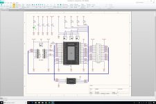
On the attached schematic, we have 5 pins on the J1 and J2 connectors that should not be connected to anything. Is there a proper way in Altium Designer/CircuitStudio to mark them as purposefully unconnected? I remember that Eagle does that with a red cross, but this is the symbol that Altium uses for connection points, therefore it would not be appropriate here.
On the attached schematic, we have 5 pins on the J1 and J2 connectors that should not be connected to anything. Is there a proper way in Altium Designer/CircuitStudio to mark them as purposefully unconnected? I remember that Eagle does that with a red cross, but this is the symbol that Altium uses for connection points, therefore it would not be appropriate here.
Attachments
Schottky Diodes for Debouncing
After a long day of work, I have identified almost all the components that I need for the encoder with LED ring. The only ones missing are the Schottky Diodes used for debouncing (D1, D2, and D3 on this schematic). Not fully understanding how this part of the circuit is supposed to work, I cannot define the required specifications for these diodes. Any suggestion?
After a long day of work, I have identified almost all the components that I need for the encoder with LED ring. The only ones missing are the Schottky Diodes used for debouncing (D1, D2, and D3 on this schematic). Not fully understanding how this part of the circuit is supposed to work, I cannot define the required specifications for these diodes. Any suggestion?
Attachments
You don't really need the diode, I think, but practically any general purpose diode will work here.
Debouncing, hardware and software, part 2
I think this technique is Figure 3.
Debouncing, hardware and software, part 2
I think this technique is Figure 3.
You don't really need the diode, I think, but practically any general purpose diode will work here.
Debouncing, hardware and software, part 2
I think this technique is Figure 3.
I read that article as well. Really good stuff...
What's making the diode selection difficult is that I don't know what I don't know, therefore I'm afraid of picking one that would not work for some reason. The range of options is quite large (Cf. search results). In particular, I am not sure which values I should target for these:
- Forward Current
- Forward Voltage
Any idea?
The current is going to be small in this application. The forward voltage probably just needs to be reasonably low, I'd have to give it more thought, but probably anything short of a very high Vf diode combined with low VCC will work.
Try this:
SD0603S040S0R2 AVX | Mouser
The current rating is probably overkill but the package is 0603 and has fully metallized terminals unlike some surface mount diodes, so it's easy to hand solder.
You have to be kidding me! MikroE just came back and indicated that the diodes are... the SD0603S040S0R2!
Now you can call me impressed...
That being said, thank you so very much for your help. MikroE's confirmation is just that. But what I get out of this thread is totally priceless.
Chris, you rock!
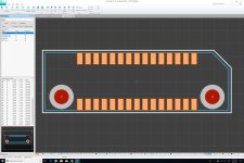
Schottky Diode
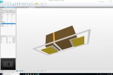
Here is the footprint and 3D body for the much sought after SD0603S040S0R2 Schottky diode. The 3D body isn't a great representation of the actual part, but it's the best I could find. Fortunately, we managed to find 3D bodies for all the parts that will be used. As soon as we're done with the schematic, we'll get going with the PCB layout. In my opinion, this is the fun part.
Here is the footprint and 3D body for the much sought after SD0603S040S0R2 Schottky diode. The 3D body isn't a great representation of the actual part, but it's the best I could find. Fortunately, we managed to find 3D bodies for all the parts that will be used. As soon as we're done with the schematic, we'll get going with the PCB layout. In my opinion, this is the fun part.
Attachments
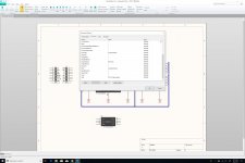
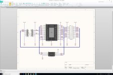
First Schematic for Base Board
Here is the first complete schematic for the base board of the E1 single encoder with LED ring brick. We're going to make a few changes before working on the PCB though. The encoder that we had selected (EC11J1524413) requires a non-round hole, which is not supported by CircuitStudio. Furthermore, it's a rather exotic surface mount version, and I am a bit concerned by its reliability. Instead, we'll go for a more standard through-hole version.
Here is the first complete schematic for the base board of the E1 single encoder with LED ring brick. We're going to make a few changes before working on the PCB though. The encoder that we had selected (EC11J1524413) requires a non-round hole, which is not supported by CircuitStudio. Furthermore, it's a rather exotic surface mount version, and I am a bit concerned by its reliability. Instead, we'll go for a more standard through-hole version.
Attachments
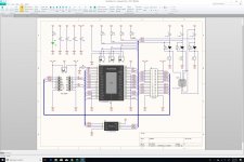
Here is the first complete schematic for the base board of the E1 single encoder with LED ring brick. We're going to make a few changes before working on the PCB though. The encoder that we had selected (EC11J1524413) requires a non-round hole, which is not supported by CircuitStudio. Furthermore, it's a rather exotic surface mount version, and I am a bit concerned by its reliability. Instead, we'll go for a more standard through-hole version.
I take that back, the EC11J1524413 simply requires two round holes drilled next to each other in order to form an oblong hole. Nevertheless, since the base board requires through hole headers for the mikroBUS connector, we should go for an encoder mounted with through holes as well: the EC11K1524406 should do the job just fine.
- Home
- Source & Line
- Digital Line Level
- 8 × AK5578EN + 8 × AK4499EQ ADC/DAC Boards