More Click Boards on Order
We've ordered a few more Click Boards. The ADAC Click with AD5593R 8-Channel, 12-Bit, configurable ADC/DAC with on-chip reference and I²C interface should be especially interesting to play with.
We've ordered a few more Click Boards. The ADAC Click with AD5593R 8-Channel, 12-Bit, configurable ADC/DAC with on-chip reference and I²C interface should be especially interesting to play with.
Alternative to TLV320AIC34
I was planning to use the TLV320AIC34, but the TLV320AIC34EVM-K is marked as "End of Life" by Mouser. Is the CODEC being phased out as well? Any recommendation for an alternative 4-channel CODEC? Anyone has experience with the AK4627VQ?
I was planning to use the TLV320AIC34, but the TLV320AIC34EVM-K is marked as "End of Life" by Mouser. Is the CODEC being phased out as well? Any recommendation for an alternative 4-channel CODEC? Anyone has experience with the AK4627VQ?
One of the most critical components of our submodular architecture (USB + mikroBUS) in the context of modular audio synthesis is the P4 brick, which is supposed to offer four hybrid AC/CV ports. This brick is used by 20 of the 23 instruments that we are planning to build. This is a challenging brick to design, because each of its four TRS ports will need to carry a wide range of mutually-exclusive signals (on the left channel, the right one being used for the signal's digital signature):
- Audio input (-5V to +5V)
- Audio output (-5V to +5V)
- Control input (-2.5V to +2.5V or 0V to 8V)
- Control output (-2.5V to +2.5V or 0V to 8V)
- Trigger, gate, or clock input (0 to 5V)
- Trigger, gate, or clock output (0 to 5V)
The audio inputs/outputs do not need to be of super high quality, but 24-bit/94kHz with decent SNR would be nice. For four channels, we could use something like the TLV320AIC34. The control inputs/outputs do not need more than 12 bits, therefore something like the AD5593R would be great (even though it would waste 4 of its 8 channels).
What makes the design difficult is that we want any port to be either an input or an output, for audio or for control, on demand. This is particularly challenging because audio and control ports require different voltage ranges, while Eurorack is not backed by a solid specification. As a result, different vendors of Eurorack modules implement the standard in different ways, which prompted the writing of this kind of alternative specification (which does not seem to be gaining much traction).
Ideally, we could do everything with a single chip, using an audio chip like the TLV320AIC34 to handle both audio and control ports, but I am not sure how to address the issue of different voltage ranges. And we will want to make sure that our ports are well-enough protected to support patching from external Eurorack modules that might have taken the original specification a bit too liberally.
Bottomline: we are still not sure what to do there...
I forgot to mention that carrying four digital audio channels (inputs or outputs) on the mikroBUS will be a bit of a challenge. And I'm not even sure that it is possible quite frankly...
Rotary Encoder
Here is the Click Board which design we are planning to use for our E1 brick (single encoder with LED ring). The beauty of the MikroE platform is that each Click Board comes with a microSDK package available for 7 different platforms and for three different compilers (C, Basic, Pascal), alongside a sample application. This makes early prototyping super easy. The only challenges that I encountered were that I had to manually enter one path for a library, and comment out some logging commands for which an initialization variable could not be resolved (I am still trying to figure out why).
That being said, this little test shows that building our E1 brick won't be trivial, because with the sample code that I am using, the encoder easily skips some detents when rotated a bit too fast. I will play with different delay values, but this is a great example of the kind of challenges that we will face: this type of problem could come from the hardware, the protocol in use, the MCU, or the software, and fixing little details like that could keep us busy for a while. But this is all part of the fun I guess...
Attachments
AK4499EQ Evaluation Board Coming
Thanks to the very timely advice of an angel, I just snatched one of the two AK4499EQ Evaluation Boards that were available on DigiKey this morning. As of this writing, one still remains. At $600, it's not exactly a bargain, but I was actually expecting something in the range of $800 to $1,000, so I'm rather happy. Overnight delivery should bring it to my doorstep by tomorrow morning.
The long wait is about to end, and the real work will soon begin...
Thank you angel!
Rotary Encoder
I have played a bit more with the code for the Knob G Click and managed to make it a bit more responsive, first by removing the logs, second by removing the Delay_1ms() calls. The former should not be a problem, but I'm not sure the latter is such a good idea. Also, thanks to MikroE's technical support (which is outstanding btw), I fixed the problem with the logs: all that was required was to replace _LOG_USBUART_A with _LOG_USBUART. This was due to the fact that I am using a brand new development board, while the sample code for the encoder was written for an older one. I am still trying to find a proper technical documentation for the new board though.
I have played a bit more with the code for the Knob G Click and managed to make it a bit more responsive, first by removing the logs, second by removing the Delay_1ms() calls. The former should not be a problem, but I'm not sure the latter is such a good idea. Also, thanks to MikroE's technical support (which is outstanding btw), I fixed the problem with the logs: all that was required was to replace _LOG_USBUART_A with _LOG_USBUART. This was due to the fact that I am using a brand new development board, while the sample code for the encoder was written for an older one. I am still trying to find a proper technical documentation for the new board though.
First Sub-Project
For us to stand even of remote chance of pulling this massive project off, we need to break it down into multiple pieces, and we need to start small, make a lot of mistakes, learn from them, and carry on. With that in mind, we have decided what the first sub-project will be: the E1 brick (single encoder with LED ring).
This is a small-enough project that we can hope to make it work in a relatively short timeframe. By the same token, it's an exciting-enough project to keep us motivated. Of course, we could do an even simpler project like the B1 single button brick, but there is not very much fun in it.
This brick will be based on the Knob G Click, but will preserve a mikroBUS S-size (unlike the L-size of the Knob G). To achieve this, it will be made of two PCBs, one hosting the EC11J1524413 rotary encoder and PCA9956B 8-bit, 24-channel, constant current LED driver, and the other hosting the 24 LEDs.
While we are using a slightly different encoder compared to the Click Board (SMD mount, metal shaft, longer operating life), we are sticking to the same LED driver. This will ensure that we can reuse the mikroSDK library that we are using for the Click Board. Once we are successful with this project, we will consider doing one with 32 RGB LEDs.
The reason why we have to use two PCBs is that the smallest SMD rotary encoders that we could find (from Alps or Bourns) have a 19mm × 16.5mm footprint on the board, which means that there is no room to fit the LEDs around them. As a result, we need to put the LEDs on a mezzanine board that will be connected to the mikroBUS add-on board through a pair of Hirose connectors. The mezzanine board will have a 10mm round hole in the middle in order to let the rotary encoder's shaft through.
With that approach, our brick will remain 100% compatible with the mikroBUS specification.
The aim of this project is to give us:
- a first opportunity to learn our selected EDA tool.
- a first experience in developing a main board with mezzanine board.
- a first experience with SMD-only components.
This should be fun...
Last edited:
A brief update on AK4499 eval board subjective findings to date:
https://www.diyaudio.com/forums/digital-line-level/314935-es9038q2m-board-477.html#post5870825
https://www.diyaudio.com/forums/digital-line-level/314935-es9038q2m-board-477.html#post5870825
A brief update on AK4499 eval board subjective findings to date:
https://www.diyaudio.com/forums/digital-line-level/314935-es9038q2m-board-477.html#post5870825
Thanks a lot for the link. But most importantly, thanks a lot for doing all this work and sharing it with the rest of us...
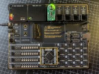
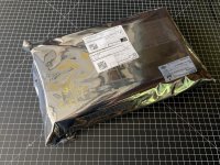
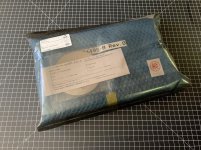
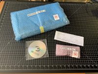
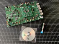
AK4499EQ Evaluation Board Received
I just received my long-awaited AK4499EQ evaluation board. The packaging is really well done, and the board is much, much bigger than I was expecting. It's also very well built, and it came with the AKDUSBIF-B interface, which I did not expect.
Now, I need to let it rest on my workbench for a while, because the last thing I want is to fry this baby with the wrong power supply...
Attachments
Altium CircuitStudio
I have spent a fair amount of time watching online tutorials for Altium CircuitStudio, and I am sold. The user interface is a lot more modern than anything else I have seen so far, and looks awesome on my new PC (192 PPI). While not cheap, it's a lot more affordable than Altium Designer, while preserving all the essential features (as far as a newbie like me can tell, ymmv). And since I am planning to spend a fair amount of time in front of that tool, a good-quality user interface really matters to me... Last but not least, learning the ropes on this entry-level tool should make it a lot easier to upgrade to Altium Designer when (if) I really need it.
I have spent a fair amount of time watching online tutorials for Altium CircuitStudio, and I am sold. The user interface is a lot more modern than anything else I have seen so far, and looks awesome on my new PC (192 PPI). While not cheap, it's a lot more affordable than Altium Designer, while preserving all the essential features (as far as a newbie like me can tell, ymmv). And since I am planning to spend a fair amount of time in front of that tool, a good-quality user interface really matters to me... Last but not least, learning the ropes on this entry-level tool should make it a lot easier to upgrade to Altium Designer when (if) I really need it.
Attachments
PCB Assembly Service Provider
Any recommendation for a reliable PCB assembly service provider? Ideally, I would like one in the US, otherwise China.
Any recommendation for a reliable PCB assembly service provider? Ideally, I would like one in the US, otherwise China.
If you plan to get a lot of use out of it, you might want to buy a single perpetual license of Altium when it goes on "sale". They usually run them every few months, I think. You get a significant discount for trading in another tool, not sure what kind of proof you have to show, but you could possibly claim to be using Eagle or KiCad.
I've never used CircuitStudio and I'm not familiar with its limitations, so hard to say if you would benefit from the full product.
For an assembly house, I have used several at work and had the most luck with Screaming Circuits. They are probably not the cheapest, though. They are ok if you don't have a lot of special instructions and don't mind if it's a day late. Honestly, we have had minor issues of one type or another with every single assembly house we've tried.
Last edited:
If you plan to get a lot of use out of it, you might want to buy a single perpetual license of Altium when it goes on "sale". They usually run them every few months, I think. You get a significant discount for trading in another tool, not sure what kind of proof you have to show, but you could possibly claim to be using Eagle or KiCad.
I've never used CircuitStudio and I'm not familiar with its limitations, so hard to say if you would benefit from the full product.
For an assembly house, I have used several at work and had the most luck with Screaming Circuits. They are probably not the cheapest, though. They are ok if you don't have a lot of special instructions and don't mind if it's a day late. Honestly, we have had minor issues of one type or another with every single assembly house we've tried.
Thanks a lot for the recommendation, I will give them a shot.
And I'll keep an eye on Altium promos. That being said, if you stumble upon one, please give me a nudge.
Altium CircuitStudio User Interface
I must say that I am really impressed by CircuitStudio's user interface: it's a lot more polished than anything I've used so far... And the level of configurability is great. I especially like the Inspector for editing multiple objects. This makes it a lot easier to create a custom look and feel for a component's schematic.
I must say that I am really impressed by CircuitStudio's user interface: it's a lot more polished than anything I've used so far... And the level of configurability is great. I especially like the Inspector for editing multiple objects. This makes it a lot easier to create a custom look and feel for a component's schematic.
Attachments
I am generally confused as to how you think this all works. Mark doesn't agree with you either, unless I am misunderstanding him. Not that it matters, because this isn't a matter of opinion. Go ask AKM or something. This discussion is getting old fast.
You seem to have a habit of completely misunderstanding things and it is getting old fast because I never said that Mark agreed with me.
What I said was that Mark understood what it was I was trying to say. You, on the other hand, most certainly did not.
When Mark said this...
Chris,
I think maybe some of the problem above has to do with how the clocking hand off from LRCK in the case of PCM, or BCLK in the case of DSD, gets passed over to MCLK. In other works if MCLK is at arbitrary phase with whatever input clock is used, how is it guaranteed there isn't false triggering at the hand off due to simultaneous clock edges.
That's exactly what it is I've been trying to say.
No, no, no... conversion is not triggered by LR clock. It is triggered by MCLK. It is not even possible for it to have been triggered by LR clock when the converter rate is much higher than this.
This makes no sense and I don't think you understand what I mean by being triggered, even though I went out of my way to specifically describe it. Just because the LR clock is running slower than the master clock does NOT prevent it from being used as a trigger, or a flag, by which to initiate the conversion process.
By definition the edge of the LR clock changes when the entire 64 bit word has been entered into the input register of the DAC. Before this happens there is no data for the DAC to process and once the LR edge changes there is. So as soon as the edge changes on the LR clock the DAC now knows there's data for it to convert and a flag is probably set in hardware, most likely upon the LR clock changing state, letting the system know that the input register is full and data conversion can begin.
Something is used to let the DAC know the exact moment that it contains data in its input register and that it can convert it analogue.
I think you have a large misunderstanding somewhere, maybe in how digital works. How could jitter on the DATA signal do anything?.
You've not understood what it is I've been trying to say.
Data starts entering the DAC > The LR clock goes through the appropriate transition indicating that there's data to be processed > This transition sets an internal flag within the DAC saying conversion can begin > The DAC starts conversion (obviously run by the master clock) > An analogue voltage is created a few moments later to the tune of the DACs internal group delay.
The master clock on its own contains no information about when there's data to be processed. That happens when the LR clock changes state. When it changes state the DAC then knows there's data to convert and conversion will begin.
If with each consecutive data byte conversion is initiated by the LR changing state, then jitter on the LR would matter.
Sample 1) - LR state change indicating there's data and for conversion to begin > DAC group delay > analogue voltage.
Sample 2) - LR state change indicating there's data and for conversion to begin > DAC group delay > analogue voltage.
Sample 3) - LR state change indicating there's data and for conversion to begin > DAC group delay > analogue voltage.
The place in time that the samples would appear on the output of the DAC, as a voltage, would be controlled by the change in state on the LR clock setting the *data is present, begin conversion flag* at the start of the conversion process. Jitter present on the LR clock would therefore alter the the time that this flag gets set between samples. As the DAC group delay remains constant, the analogue voltage would be distorted due to the changes in voltage (dictated by each new sample) arriving before/after they should.
When Mark said this...
Chris,
I think maybe some of the problem above has to do with how the clocking hand off from LRCK in the case of PCM, or BCLK in the case of DSD, gets passed over to MCLK.
It's this hand off that I am talking about. The data clocks clearly indicate to the DAC when the data is present and will trip some sort of interrupt flag, or similar, upon a data byte being transferred and that data conversion can begin. Conversion will be handled by the master clock, but if the timing from the LR clock, that sets the start of the conversion flag, finds its way, in any shape or form, to the output of the DAC, then jitter present there, would matter.
Now that ESS paper I linked to, earlier on, goes to a lot of trouble to describe their method of removing jitter from the data lines and giving you the impression that doing so is very important. You are saying otherwise though. So are ESS lying about this?
Obviously they are using an ASRC and are reclocking all of the data to the tune of a new, very low jitter, master clock. But if what you are saying is true, then the reason for doing so is to eliminate jitter present on the old master clock, not to remove jitter from the incoming data lines. If this is the case then why do ESS describe the process as removing jitter from the data? 😕
You seem to have a habit of completely misunderstanding things and it is getting old fast because I never said that Mark agreed with me.
What I said was that Mark understood what it was I was trying to say. You, on the other hand, most certainly did not.
When Mark said this...
That's exactly what it is I've been trying to say.
This makes no sense and I don't think you understand what I mean by being triggered, even though I went out of my way to specifically describe it. Just because the LR clock is running slower than the master clock does NOT prevent it from being used as a trigger, or a flag, by which to initiate the conversion process.
By definition the edge of the LR clock changes when the entire 64 bit word has been entered into the input register of the DAC. Before this happens there is no data for the DAC to process and once the LR edge changes there is. So as soon as the edge changes on the LR clock the DAC now knows there's data for it to convert and a flag is probably set in hardware, most likely upon the LR clock changing state, letting the system know that the input register is full and data conversion can begin.
Something is used to let the DAC know the exact moment that it contains data in its input register and that it can convert it analogue.
You've not understood what it is I've been trying to say.
Data starts entering the DAC > The LR clock goes through the appropriate transition indicating that there's data to be processed > This transition sets an internal flag within the DAC saying conversion can begin > The DAC starts conversion (obviously run by the master clock) > An analogue voltage is created a few moments later to the tune of the DACs internal group delay.
The master clock on its own contains no information about when there's data to be processed. That happens when the LR clock changes state. When it changes state the DAC then knows there's data to convert and conversion will begin.
If with each consecutive data byte conversion is initiated by the LR changing state, then jitter on the LR would matter.
Sample 1) - LR state change indicating there's data and for conversion to begin > DAC group delay > analogue voltage.
Sample 2) - LR state change indicating there's data and for conversion to begin > DAC group delay > analogue voltage.
Sample 3) - LR state change indicating there's data and for conversion to begin > DAC group delay > analogue voltage.
The place in time that the samples would appear on the output of the DAC, as a voltage, would be controlled by the change in state on the LR clock setting the *data is present, begin conversion flag* at the start of the conversion process. Jitter present on the LR clock would therefore alter the the time that this flag gets set between samples. As the DAC group delay remains constant, the analogue voltage would be distorted due to the changes in voltage (dictated by each new sample) arriving before/after they should.
When Mark said this...
It's this hand off that I am talking about. The data clocks clearly indicate to the DAC when the data is present and will trip some sort of interrupt flag, or similar, upon a data byte being transferred and that data conversion can begin. Conversion will be handled by the master clock, but if the timing from the LR clock, that sets the start of the conversion flag, finds its way, in any shape or form, to the output of the DAC, then jitter present there, would matter.
Now that ESS paper I linked to, earlier on, goes to a lot of trouble to describe their method of removing jitter from the data lines and giving you the impression that doing so is very important. You are saying otherwise though. So are ESS lying about this?
Obviously they are using an ASRC and are reclocking all of the data to the tune of a new, very low jitter, master clock. But if what you are saying is true, then the reason for doing so is to eliminate jitter present on the old master clock, not to remove jitter from the incoming data lines. If this is the case then why do ESS describe the process as removing jitter from the data? 😕
Just. Give. Up.
The LRCK is not a critical clock and does not drive data conversion in these DACs. MCLK or divided MCLK does which is why it is required to be synchronous with the other I2S clocks.
I am not going to debate this any further. You are just plain wrong and your arguments from authority and other half baked understandings don't help. If you don't understand how jitter on DATA is completely irrelevant, then we can't even have further discussion because you don't understand the very basics.
Let's make it even more simple.
True or False questions.
1. The output of the delta sigma modulator (which is in the digital domain fully) feeds the actual D->A converter block in the chip?
2. The output of the modulator is running at an oversampled rate with smaller word size than the input PCM?
If these two things are true, it does not matter what the flow was before.
Supplier Integration
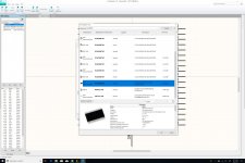
The supplier integration within Altium CircuitStudio is positively first class. Here, I am using it with Mouser, and it is making the creation of a BOM a lot easier than using a spreadsheet. Also, I am finding the official video tutorials produced by Altium to be quite effective. They're very short and super fast (you kinda need to play them in stop motion), but they allow me to get the job done.
So far, I'm loving it...
Attachments
Last edited:
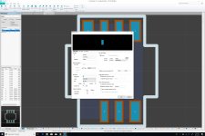
Question about solder paste and solder land
I am a bit confused about how to properly implement the footprint described on Page 3/5 of the following datasheet. For the bottom left pad, the solder paste area is 0.3mm × 0.65mm, while the solder land area is 0.4mm × 0.75mm. First, I am assuming that the solder land area is equivalent to the area occupied by the copper pad, but is that really the case? Second, how am I supposed to implement that in Altium CircuitStudio? I have attached a screenshot showing what I did, but it does not seem right:
- 0.3mm × 0.65mm pad
- 0.05mm Solder Mask Expansion
Furthermore, what does "Top Solder" mean? Is that again equivalent to what the Nexperia datasheet calls "solder land"?
A detailed documentation of the terminology used by Altium for the different layers would be useful, but I could not find any that clearly answered my questions.
Attachments

Last edited:
- Home
- Source & Line
- Digital Line Level
- 8 × AK5578EN + 8 × AK4499EQ ADC/DAC Boards