Cortez, in Class II equipment, like power amps and PCs, the GNDs are (nearly) always connected to PE.
Don't to forget those sneaky ones like printers and TVs that could be connected to a system.
Don't to forget those sneaky ones like printers and TVs that could be connected to a system.
Last edited:
So PSU return current has to flow along the signal ground wires, in roughly the opposite direction to the signal?Cortez said:Yeah but I said that the signal GNDs are not connected to the PS GND on the amp PCBs.
Surely in most (or all?) Class II equipment there is no PE? Isn't that the point of Class II? Of course, there may be somewhere else in the system a Class I item which provides a PE ground for the signal.Mark Whitney said:Cortez, in Class II equipment, like power amps and PCs, the GNDs are (nearly) always connected to PE.
Yeah but I said that the signal GNDs are not connected to the PS GND on the amp PCBs.
Well then where are they connected?
Yeah, I guess I should rephrase my point: it's a good thing for safety but can casue a lot of trouble with hifi... 😛Cortez, in Class II equipment, like power amps and PCs, the GNDs are (nearly) always connected to PE.
Don't to forget those sneaky ones like printers and TVs that could be connected to a system.
I don't connect my amps to the PE at all, the mains will never get to the metal parts...
So PSU return current has to flow along the signal ground wires, in roughly the opposite direction to the signal?
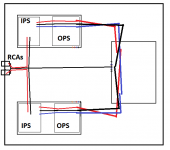
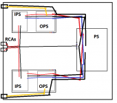
Maybe the 1st picture was not clear enough. Is this 2nd one better?Well then where are they connected?
- all PS wires goes as marked with the red, blue, black wires
- signal GNDs are going directly to the amp PCBs and they are NOT connected here to the local PS GND
- but only 1 wire goes to the RCA GND to the main GND
- if I am right no GND loop is created and the amp's inputs are directly driven without 15R resistors or anything else
- but this is just an idea I shared and did not tested in real life...!
Attachments
And I would place the speaker output termnal to the side
and then there is no crosstalk with the RCAs.
Their wires could go as it's shown with the orange wire
and with a separate GND wire going directly to the main PS GND.
Near to the OPS PS wires to create a smallest loop as possible.
BTW: the output zobel can be put even without a GND using the rails if needed!
Attachments
RCA GNDs: they are typically already connected to each other outside the amp at the source side.
So I just made a common point inside the amp to close the "loop" and bring it to the main GND as directly as possible.
To the PSU: just to equalize the 2 different GNDs (CD player + amp) to the same potential.
But with this layout I am not sure how important is the resistance of that wire...
If the 2 devices are once at the same potential how much current there will be when they are working?
Maybe some small differences due to some capacitive charging but nothing else, but I am not sure...
You should not connect the RCA's like that Cortez.
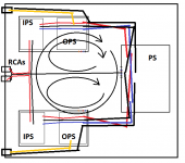
You should take them both to the PCB (both the signal wire and its return) and there should be no connection from the RCA to the central star ground from where the RCA's are located on the back panel. If you do this the way you show, you have created a big loop, and any stray flux (i.e. transformer field or signal field e.g. from the output) will induce an error voltage = potential hum and/or distortion.
From what I can see, it looks like you have routed your speaker return wire back next to the output lead and into the main PCB module wire bundle. This looks good - you have kept the output wiring loop area small.
I dont get it: where is the GND loop here?
(Again: the signal GNDs are NOT connected to the local PS GNDs on the amp PCB!)
RCA: both the GND and the "hot" wire as a pair of wires are going to the PCB!
(Black wire = signal GND, Red wire = signal "hot" wire)
And if so: there is no loop but not even a signal GND - PS GND connection so that's why
that one wire goes between this 2 nodes without creating a loop as in any other cases
(maybe "corrected" with some series resistor which I see as a 2nd best solution only...)
Untill the signal GND doesnt create a loop I guess this is not a problem.
PS wiring is often implemented like on this picture without casuing any hum problem.
But I guess lets stop discussing too much about this... It would be quicker to try it then discuss in mind simulation... 😀
And anyways it was just a thoretical idea I shared, maybe it has some potential... That's all folks... 😉
Last edited:
I dont get it: where is the GND loop here?
(Again: the signal GNDs are NOT connected to the local PS GNDs on the amp PCB!)
RCA: both the GND and the "hot" wire as a pair of wires are going to the PCB!
(Black wire = signal GND, Red wire = signal "hot" wire)
And if so: there is no loop but not even a signal GND - PS GND connection so that's why
that one wire goes between this 2 nodes without creating a loop as in any other cases
(maybe "corrected" with some series resistor which I see as a 2nd best solution only...)
Look again Cortez. They are . . .
Remember, you are working to minimize two things:-
1 loop areas
2 common impedance coupling.
Even if your RCA return is not connected at the amp PCB but to the central star ground , the induced error current will flow from the star ground to the RCA return, down the interconnect cable, out of the output of the source and back into the amplifier input, through the amp circuitry and then the PCB ground connection to the star earth.
When you wire up the way we are suggesting, you minimize the loop area inside the amplifier and therefore the loop current and the noise.
Sorry, but I still think it's OK, so untill it's tried out I reserve my right to be right (or wrong)... 😉
Leach talks about this in Lo Tim.Yeah but I said that the signal GNDs are not connected to the PS GND on the amp PCBs.
And he addresses the multiple loop problem.
The LOOP AREA must be minimised to attenuate the interference.
That requires YOU to locate the wiring so that there is LOW Loop Area.
Last edited:
Yeah, but not everything is a loop which looks like one... 🙂
(We should try it out instead of writing pages of guessing...
But unfortunately right now I don't have any amp on the bench to try with... 🙂)
(We should try it out instead of writing pages of guessing...
But unfortunately right now I don't have any amp on the bench to try with... 🙂)
Everybody has the right to be wrong, and then suffer the consequences of this: the universe can be merciless to people who include ground loops or deliberately inject buzz into a signal ground.
Sorry, but I still think it's OK, so untill it's tried out I reserve my right to be right (or wrong)... 😉
I admire your confidence.
🙂
I haven't been able to spend any time on this for a few days but certainly wasn't expecting 6 pages when I returned!
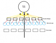
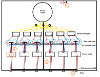
I have one very large power transformer with one + and - winding.
This feeds six separate Thyristor bridge's (so I can turn each channel off to save power)
I have 6 sets of capacitors from each Thyristor bridge.
The above is fixed, I have acquired these parts and don't intend on changing transformers or capacitors now.
I have drawn a diagram and am unsure where to go after this as there as so many different possible combinations.. I've started SIMPLE and cut out zobels, IPS boards, etc. Please could someone modify my mspaint creation to demonstrate best practice?
Do I connect the cap common points to the PE ground at all?
I have ditched the aluminium toroidal potting in favor of a 3mm steel box, moved the small toroid to the other side in my cad model and will rivet a piece of steel to the aluminium frame on this side.
Thanks
You still haven't told us how many secondaries you have, and how many rectifiers you intend to use. Unless you have separate secondaries for each amp and separate rectifiers
I have one very large power transformer with one + and - winding.
This feeds six separate Thyristor bridge's (so I can turn each channel off to save power)
I have 6 sets of capacitors from each Thyristor bridge.
The above is fixed, I have acquired these parts and don't intend on changing transformers or capacitors now.
I have drawn a diagram and am unsure where to go after this as there as so many different possible combinations.. I've started SIMPLE and cut out zobels, IPS boards, etc. Please could someone modify my mspaint creation to demonstrate best practice?
Do I connect the cap common points to the PE ground at all?
I have ditched the aluminium toroidal potting in favor of a 3mm steel box, moved the small toroid to the other side in my cad model and will rivet a piece of steel to the aluminium frame on this side.
Thanks
Attachments
Hi Matt!
My suggestion looks like this but let's wait for someone elses recommendation too... 🙂
There are 2 new wires:
Other notes marked with the orange circles and numbers:
Or you can dismiss the wire at circle #3 and use a 15R resistor to connect
the signal GND with the PS GND on every amp PCB, just as Bonsai suggested.
My suggestion looks like this but let's wait for someone elses recommendation too... 🙂
There are 2 new wires:
- a thick common GND connection for the separate PS cap banks
- and a similar to the RCAs GNDs
Other notes marked with the orange circles and numbers:
- do not connect signal GND with PS GND on amp PCB
- twist PS wires tightly from caps to amp (and from trafo to caps as well!)
- signal GND and main PS GND conenction: maybe you can place a 10R - 100R resistor here
- connect the PE to your chassis if you want
- but then isolate your RCAs from the chassis
Or you can dismiss the wire at circle #3 and use a 15R resistor to connect
the signal GND with the PS GND on every amp PCB, just as Bonsai suggested.
Attachments
- Status
- Not open for further replies.
- Home
- Amplifiers
- Solid State
- 6-channel-amplifier-grounding
