KiCAD has a steep learning curve. I'm working on everything you suggested and when time permits I'll send you some free samples.
Regards,
Dan
Regards,
Dan
Still tinkering with KiCAD and trying to make some Schade PCBs.
Regards,
Dan
I think there may be an error in your board. I believe that pin 5 (collector), not pin 6, of the 4N37 should be connected to the capacitor and 22R resistor.
KiCAD has a steep learning curve. I'm working on everything you suggested and when time permits I'll send you some free samples.
Regards,
Dan
Hi Dan
Yeah fat large track connections to IXYS.
Do 3 watts (or more) 0.2R power resistors dimensions on the pcb are OK ?Good luck to You in the learn & design 🙂
Hi Dan
Yeah fat large track connections to IXYS.
Do 3 watts (or more) 0.2R power resistors dimensions on the pcb are OK ?Good luck to You in the learn & design 🙂
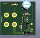
Since this is my first time doing PCBs who would like to check my designs for flaws?
Regards,
Dan
I think there may be an error in your board. I believe that pin 5 (collector), not pin 6, of the 4N37 should be connected to the capacitor and 22R resistor.[/QUO
Very good point!
http://www.vishay.com/docs/81181/4n35.pdf
Regards,
Dan
Last edited:
Hi Dan
Yeah fat large track connections to IXYS.
Do 3 watts (or more) 0.2R power resistors dimensions on the pcb are OK ?Good luck to You in the learn & design 🙂
4mm
4mm only?
It's the power resistor diameter?
Probably ok if is stuffed on the PCB in vertical position.
The best starting point is after You ready have all components:
input transformers, resistors, polarized capacitors and film caps for bypass, Opto, mosfets collected on the bench.
No surprise if some components are not in stock and the others have different size. 🙂 Best regards
4mm only?
It's the power resistor diameter?
Probably ok if is stuffed on the PCB in vertical position.
The best starting point is after You ready have all components:
input transformers, resistors, polarized capacitors and film caps for bypass, Opto, mosfets collected on the bench.
No surprise if some components are not in stock and the others have different size. 🙂 Best regards
I used the following, PCB Printed Circuit Board File Creation Calculator | Advanced Circuits
Regards,
Dan
Since this is my first time doing PCBs who would like to check my designs for flaws?
Regards,
Dan
Not necessarily fixes of flaws, but merely some suggestions - I'm also just a diyer, definitely not educated in electronics but have done some reading, never designed a printed circuit board, but I have wired point to point circuits on boards:
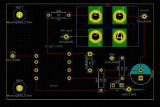
1. Take J2 off the end of resistor R5 instead of off pin 4 of 4N37.
2. You can keep traces on the bottom of the board if you move the trace that is between the IXFN drain (3) and R1. From drain (3), run trace from the lower side of (3) horizontally between (1) and (2), and then turn up to R1 (on the bottom of the board).
3. For +60V power, enter board to the left of R2 and above drain (3), and go directly to (3).
4. It is my understanding that a ground return should be provided next to the power wire (twisted) to minimize loop area and therefore noise. So I suggest you bring your 60V and ground wires twisted together to the board. If all of the circuit traces are on the bottom of the board, you can then put a ground on the top side, entering next to the 60V, then down over the IXFN, and then horizontally across and exit near J2 and J3. You might need to enlarge the space for R4 and R5 anyways so then there is room to bring a wide ground trace across under the resistors to the right side of the board. You can then continue ground wires with the power and signal out wires at J2 and J3, again twisted together to minimize loop area.
This is a good read for minimizing noise. It is by diyAudio member Bonsai:
http://hifisonix.com/wordpress/wp-content/uploads/2019/02/Ground-Loops.pdf
It is a long read, but the practical information is towards the end. I have found it very helpful and I try to follow his recommendations. In all my amps I have ground and power wires twisted together, and signal ground wires twisted together, with the goal to minimizing loop areas. All my amplifiers are quiet with my 103 dB speakers.

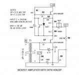
max swing/(R9+R6)=Ipp
say 60Vpp ( just to have round figure)
60Vpp/(220+22)R= 248mA
P=I^2 x R , but you need to translate Ipp to Irms , so to speak (recalculate AC to DC ,effectively) so Ipp/2/1.41 = 87mA
dissipation in resistors:
for 220R= 87mA^2 x 220R=1W69
for 22R = 0W169
so , 220R - use 3Watter
for 22R - use whateverWatter
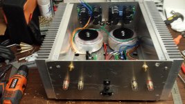
Finally made some progress. Put together to see how it all fits. Panels still have plastic coating.
Case is always the toughest part.
Built this one with just a cordless drill. 😉
That amplifier looks like serious business! I like the aluminum plate used for the panels.
You may have talked about this earlier, but are you going to use the heat sinks passively or with fans? I seem to recall dissipation is ~180W a side, a lot for even the biggest passive heat sinks.
You may have talked about this earlier, but are you going to use the heat sinks passively or with fans? I seem to recall dissipation is ~180W a side, a lot for even the biggest passive heat sinks.
This is a smaller 25w version.
max swing/(R9+R6)=Ipp
say 60Vpp ( just to have round figure)
60Vpp/(220+22)R= 248mA
P=I^2 x R , but you need to translate Ipp to Irms , so to speak (recalculate AC to DC ,effectively) so Ipp/2/1.41 = 87mA
dissipation in resistors:
for 220R= 87mA^2 x 220R=1W69
for 22R = 0W169
so , 220R - use 3Watter
for 22R - use whateverWatter
Trying to figure this out so I can determine what trace width I need on the PCBs I’m designing.
Regards,
Dan
In post #49, Pico mentioned a trim pot might be needed. What are we adjusting for?
Finished the amp today and brought it up slowly with a variac. Nothing blew up or smoked, but getting a few volts under rail voltage at the drain of the lower mosfet. Raising the bias 2 volts didn't change anything. No warm up on heat sink.
Rail - 41v
Volts at drain- ~38V
No change at drain adjusting bias
No change at drain adjusting trimmer above opti-coupler.
Results are same on both channels.
I have a lm317 voltage regulator for bias and grounded it at main circuit ground point. That ok?
Using fairchild irf9140 mosfets.
Ran out of time today but will mark a copy of the schematic with reading when I get a chance.
Thanks
Vince
......
Ran out of time today but will mark a copy of the schematic with reading when I get a chance.
....
please
Not necessarily fixes of flaws, but merely some suggestions - I'm also just a diyer, definitely not educated in electronics but have done some reading, never designed a printed circuit board, but I have wired point to point circuits on boards:
1. Take J2 off the end of resistor R5 instead of off pin 4 of 4N37.
2. You can keep traces on the bottom of the board if you move the trace that is between the IXFN drain (3) and R1. From drain (3), run trace from the lower side of (3) horizontally between (1) and (2), and then turn up to R1 (on the bottom of the board).
3. For +60V power, enter board to the left of R2 and above drain (3), and go directly to (3).
4. It is my understanding that a ground return should be provided next to the power wire (twisted) to minimize loop area and therefore noise. So I suggest you bring your 60V and ground wires twisted together to the board. If all of the circuit traces are on the bottom of the board, you can then put a ground on the top side, entering next to the 60V, then down over the IXFN, and then horizontally across and exit near J2 and J3. You might need to enlarge the space for R4 and R5 anyways so then there is room to bring a wide ground trace across under the resistors to the right side of the board. You can then continue ground wires with the power and signal out wires at J2 and J3, again twisted together to minimize loop area.
This is a good read for minimizing noise. It is by diyAudio member Bonsai:
http://hifisonix.com/wordpress/wp-content/uploads/2019/02/Ground-Loops.pdf
It is a long read, but the practical information is towards the end. I have found it very helpful and I try to follow his recommendations. In all my amps I have ground and power wires twisted together, and signal ground wires twisted together, with the goal to minimizing loop areas. All my amplifiers are quiet with my 103 dB speakers.
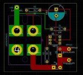
How's this?
Regards,
Dan
Attachments
- Home
- Amplifiers
- Pass Labs
- 50w Single-Ended BAF2015 Schade Enabled