Bensen,
Thank you for continuing to share your ideas and progress. Using the wooden power supply test board for the first amplifier prototype is an efficient strategy. You can easily test improvement ideas before any chassis metal work is started. Have you considered putting the regulated driver power supply on the driver circuits PCB? Not the bridge rectifiers and transformers, just the regulator and capacitors. A single star ground must still be maintained: wires or short bus_bar
Two ideas for large Sanken packages:
1) Instead of trying to align all of the package screw holes, you can use a long square aluminum "pressure bar" that goes in back of all of the transistors and only screw this bar into the heatsink. A screw between each Sanken package. Easier assembly. Easier repair/rebuild. Some additional heat removal.
2) For a Vbe multiplier bias circuit, you can "wrap" the collector lead of a few Sanken transistors around a diode for modestly-quick thermal time constant monitoring. Thermal grease helps. Teflon/plastic tube on the diode leads helps to prevent electrical shorts. There are physically small diodes with good thermal conductivity.
Front End build = oscillations
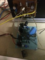
The front End and driver section is finally build. (became a father for the second time a month ago).
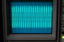
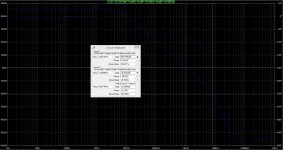
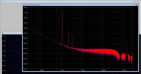
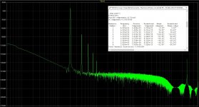
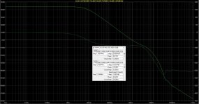
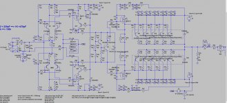
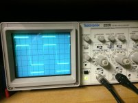
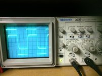
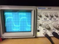
During measuring I noticed a 40Mhz oscillation with a Vpp of about 250mV (see scope picture). The simulated AC analysis however gave me a good feeling regarding stability; 76°PM and 20dB gain margin (see 2nd picture). Again a good example between a simmed and build circuit, certainly when mosfet models are used.
However, now I know I have stability issues I have to solve them. After looking at Classé and parasound circuits, the main differences are:
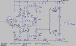
1. higher freq compensation value for capacitor from VAS output to diff input
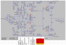
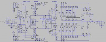
(I'm using 5pf, see picture circuit AS BUILD)
2. much higher values for feedback resistors 100K vs 8k8 in mine. However,
spice gave me worser stability when using higher values here.
All input is highly appreciated.
The front End and driver section is finally build. (became a father for the second time a month ago).
During measuring I noticed a 40Mhz oscillation with a Vpp of about 250mV (see scope picture). The simulated AC analysis however gave me a good feeling regarding stability; 76°PM and 20dB gain margin (see 2nd picture). Again a good example between a simmed and build circuit, certainly when mosfet models are used.
However, now I know I have stability issues I have to solve them. After looking at Classé and parasound circuits, the main differences are:
1. higher freq compensation value for capacitor from VAS output to diff input
(I'm using 5pf, see picture circuit AS BUILD)
2. much higher values for feedback resistors 100K vs 8k8 in mine. However,
spice gave me worser stability when using higher values here.
All input is highly appreciated.
Attachments
Last edited:
This may be input cascode, try 47-100pF between base and collector of Q9-Q1240Mhz oscillation with a Vpp of about 250mV
Thanks alot for this tip! Did not think of that by myself. It seems to work: at the moment I have 68pF between each base and collector of the cascode bjt's and the oscillation level dropped already from 250mvpp to 20mvpp!
I used the RC combination at the bases as proposed by Bonsai in one of his excellent papers, appaerently it does not seem to work in my configuration while I tried several RC combinations whitout effect.
But how can it be that many oem's get away without this cap between base and collector at their cascodes???
Better to have R60 and R82 in each base, not shared
Different signal transfer from sources to cascode bases
Different signal transfer from sources to cascode bases
But how can it be that many oem's get away without this cap between base and collector at their cascodes???
Because they are not needed. Your C1, C2 are too low, try 100 pF trimmer caps to find sweet spot, definitely some compensation work ahead.
Last edited:
It may also potentially come from the drivers. N-channel FETs have always got lower input capacitance (Ciss), than the P-channel ones. At 70mA quiescent current it may play its role, unbalancing the driver stage at HF.
The difference is around 40pF (170 and 210 for N and P respectively), so you may want to try adding 39-47pF in addition to C18 to compensate this difference.
The difference is around 40pF (170 and 210 for N and P respectively), so you may want to try adding 39-47pF in addition to C18 to compensate this difference.
The extra cap as proposed by Dimitri has some effect, but I haven't been able to remove the oscillation completely.
Please find below some trials and their results. I'm still having 25Mhz oscillation with a 10mvpp oscillation.
All ideas are welcome!
I've tried to increase the miller cap and even remove it, the difference wasn't even visible on my scope.Because they are not needed. Your C1, C2 are too low, try 100 pF trimmer caps to find sweet spot, definitely some compensation work ahead.
This was definetely in the good direction. I've tried several values to compensate the difference between the P and N-channel device. However, the best result was to remove both capacitors.It may also potentially come from the drivers. N-channel FETs have always got lower input capacitance (Ciss), than the P-channel ones. At 70mA quiescent current it may play its role, unbalancing the driver stage at HF.
The difference is around 40pF (170 and 210 for N and P respectively), so you may want to try adding 39-47pF in addition to C18 to compensate this difference.
Please find below some trials and their results. I'm still having 25Mhz oscillation with a 10mvpp oscillation.
All ideas are welcome!
Attachments
i agree with dimitri's suggestion of 4 separate base resistors for Q9-Q12.
maybe a larger value than 22ohms, too.
it's probably a little late to bring this up; i heard of folks addressing problems like this with small resistance (5-10 ohms) in series with each J1-J4 jfet drain and it's corresponding cascode Q9-Q12 emitter.
cordell advocates series R-C at mosfet gates can help tame them.
please keep reporting on how things are going and sharing your findings. some time later this year, i hope to be experimenting with something similar.
we're cheering you on!
mlloyd1
Last edited:
drats; the editor timed out on me ...
i also wanted to mention that PMA had posted some info about a power amp he built and measured that was strongly inspired by the parasound JC-1. it is not NFB, but otherwise shares some topological similarities to your design. might be worth taking a look. i couldn't find a link to it quickly, so the editor may time out again before i do.
mlloyd1
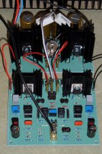
Years have passed, kids grown older (4.5 + 2.5years) and got some free time.
I've got a proto version running with 1 pair of output transistors. I only can compare it with my previous build (http://www.diyaudio.com/forums/soli...n-subwoofer-wideband-duty-13.html#post3382545) and a denon PMA700V.
This proto version "opened up" the music a lot more compared to my previous build which I found better sounding than the Denon. And keeping the same resolution and detail, I'll blame this on the Fet drivers (Profusion lateral Fets) and the Lateral mosfet Vas stage (2SK216/2SJ79).
Now I need to tweak the VBE multiplier and compensation caps.
All remarks/ proposals are welcome.
Attachments
During some stability testing and tuning the Spice Mosfet models to have datasheet like transfer curves, I've noticed excessive gain.
Apparently in this design, the drain (load) resistors from the Jfet input stage are leading in setting the OLG instead of the VAS emitter degeneration resistors. To reduce the OLG, I need to lower VAS degeneration!?
Also the total amount of frequency compensation caps could be reduced a bit more, according spice. Measurements have to confirm this.
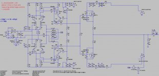
Following circuit I hope to test shortly.
Apparently in this design, the drain (load) resistors from the Jfet input stage are leading in setting the OLG instead of the VAS emitter degeneration resistors. To reduce the OLG, I need to lower VAS degeneration!?
Also the total amount of frequency compensation caps could be reduced a bit more, according spice. Measurements have to confirm this.
Following circuit I hope to test shortly.
Attachments

LineSource.
You mention "voicing". I have heard that expression before. It seems to be some sort of way to "tweak" the amplifier to perform it's best. Usually by listening tests.
The interesting thing now is what parameters are usually tweaked? Is it the various bias currents? Or perhaps the HF behavior and roll of with compensation circuitry?
The amps I have made are not really "voiced" in a rational way. It's more like some sort of long time iterative process like:
Simulation -> prototype -> listening -> some objections some weeks later -> simulations -> modification -> etc..
But since I don't like to listen to musik unless I'm in the mood, the process is quite slow. But it works.
I just will mention one thing. I think the HF behavior has a surprisingly hefty impact on the sound. Dispite we aren't bats. But often amps opens up when compensated even more than what's necessary to get a good phase margin.
Any thoughts on this?
I noticed a rather high amount of hum through my test speaker. It appeared to be a +-100Hz signal with an amplitude of +-50mVpp.
What have I done:
1. checked PSU voltage with oscope ==> all looked fine
2. tested with all kinds of small bypass caps on zeners IPS and VAS cascodes. ==> NOK (hum still present)
3. removed hawksford cascode in VAS, only Lat fets as VAS ==> NOK
4. changed hawksford casode in IPS to cascode referenced to GND ==> NOK
5. changed CCS for cascode reference IPS to series connection of resistors ==> hum decreased to 10mVpp
6. increased base stopper cascode BJT's IPS to 680Ohm ==> hum decreased to +- 1mvpp. I can hear a very very tiny hiss when keeping my ear against the speaker.
7. implemented the cascode in the VAS again, but this time no hawkford. ==> still OK.
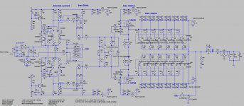
With the current status (see testing circuit below = without BJT OPS), 20kHz 30Vpp in 8Ohm//100n is as good as perfect. 100Khz square is also super (will take pictures next time!).
BUT, currently I'm having 3mA Bias current for the input Jfet and would like to increase to 7..8mA.
During increasing of IPS bias and keeping VAS bias to +-25mA and DC offset to a few mV's. Once the bias is at +-5mA, a big hum appears in my speaker and current increase everyware, is way to much.
Now, what is going on here?? I have to reduce the IPS loading resistors to maintain VAS currents, so OLG is lowering. Also Spice is not helping me to reveal this. Why it looks like the circuit is getting unstable??
What have I done:
1. checked PSU voltage with oscope ==> all looked fine
2. tested with all kinds of small bypass caps on zeners IPS and VAS cascodes. ==> NOK (hum still present)
3. removed hawksford cascode in VAS, only Lat fets as VAS ==> NOK
4. changed hawksford casode in IPS to cascode referenced to GND ==> NOK
5. changed CCS for cascode reference IPS to series connection of resistors ==> hum decreased to 10mVpp
6. increased base stopper cascode BJT's IPS to 680Ohm ==> hum decreased to +- 1mvpp. I can hear a very very tiny hiss when keeping my ear against the speaker.
7. implemented the cascode in the VAS again, but this time no hawkford. ==> still OK.
With the current status (see testing circuit below = without BJT OPS), 20kHz 30Vpp in 8Ohm//100n is as good as perfect. 100Khz square is also super (will take pictures next time!).
BUT, currently I'm having 3mA Bias current for the input Jfet and would like to increase to 7..8mA.
During increasing of IPS bias and keeping VAS bias to +-25mA and DC offset to a few mV's. Once the bias is at +-5mA, a big hum appears in my speaker and current increase everyware, is way to much.
Now, what is going on here?? I have to reduce the IPS loading resistors to maintain VAS currents, so OLG is lowering. Also Spice is not helping me to reveal this. Why it looks like the circuit is getting unstable??
Attachments
With the help of some forum members I managed to get rid of the hum completely. Main reasons for the hum were IIRC:
1. VAS cascodes
2. voltage references for JFET IPS cascodes
3. increase of drain resistors FET VAS devices
More here: Cascode JFET IPS oscillation - getting crazy
Now that this was solved I tested different VAS devices.
1. 2SK216/2SJ79 lateral Fets: Very good detail and contrast
2. 2SK2013/2SJ13 Vert audio Fets: Less detail, more muddy sound
3. IRF9610/ IRF610 Vert Fets: same as 216/79 but more musical sounding, better soundstage.
I really had in mind the 216/79 would be best, so I tested different bias currents, lowered IPS bias and increased IPS drain to resistors to increase IPS gain, played with different VAS drain/degeneration resistors. NO result was better than the 9610/610. So I left the 9610/610 in as VAS Fets and used 216/79 as IPS cascodes.
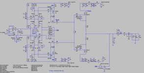
Below is current circuit, still without BJT output stage and some square wave testing 20Vpp at 20K,50K and 100Khz in 8Ohm.
1. VAS cascodes
2. voltage references for JFET IPS cascodes
3. increase of drain resistors FET VAS devices
More here: Cascode JFET IPS oscillation - getting crazy
Now that this was solved I tested different VAS devices.
1. 2SK216/2SJ79 lateral Fets: Very good detail and contrast
2. 2SK2013/2SJ13 Vert audio Fets: Less detail, more muddy sound
3. IRF9610/ IRF610 Vert Fets: same as 216/79 but more musical sounding, better soundstage.
I really had in mind the 216/79 would be best, so I tested different bias currents, lowered IPS bias and increased IPS drain to resistors to increase IPS gain, played with different VAS drain/degeneration resistors. NO result was better than the 9610/610. So I left the 9610/610 in as VAS Fets and used 216/79 as IPS cascodes.
Below is current circuit, still without BJT output stage and some square wave testing 20Vpp at 20K,50K and 100Khz in 8Ohm.
Attachments
Where do you source the TO220 lat fets..??
I like your schematic..though i believe that its a tad too complicated
I like your schematic..though i believe that its a tad too complicated
I've bought them over the years by different sources.
Some came from ebay: there still are some Original ones on ebay (look also for the 2sk213/214/215 and 2SJ76/77/78 which are lower Vds versions).
Important is that the thicker part of the legs directly under the body are clearly longer than with standard TO220 packages.
Too complicated? Personally, I don't think there are many possibilities to make it more simple than this when using the same amount of stages and IPS cascodes.
F... the vbe multiplier. Blew already 3pairs exicon lateral mosfets drivers and 2 pair 2sc2922/2sa1216 output bjt's with playing with to find a good temperature compensation.
I'm considering changing the design to bjt drivers with 6 or 8 pairs lateral mosfets. (3 or 4 pairs double fet's exicon).
Any advise?
I'm considering changing the design to bjt drivers with 6 or 8 pairs lateral mosfets. (3 or 4 pairs double fet's exicon).
Any advise?
I was using TO-220 LMOS driving Sanken LAPT 2SC2922 as you are doing. But i also developed another version that use BJTs drive Exicon LMOS output, since TO-220 LMOS currently very hard to find and the famous Sanken 2SC2922/2SA1216 are going EOL.
It's hard to say what sounding better, TO-220+Sanken BJT more treble, detail, sweet. but BJT /Exicon LMOS better in mids.
It's hard to say what sounding better, TO-220+Sanken BJT more treble, detail, sweet. but BJT /Exicon LMOS better in mids.
- Home
- Amplifiers
- Solid State
- 2nd amp from scratch: Low NFB- FET front end - BJT OPS