Will be interesting to hear what Kevin says. That part of the circuit is the Vbe mutliplier, which is used to bias the output stage. I can't see how it would possibly work the way it is currently: it must be a layout error.
OK, then I will change one tomorrow and see if that fixes it. I have extra boards if I need to go back. Like I said, these don't work so what have I got to lose?
Thanks, Terry
Thanks, Terry
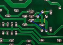
Here are the board changes that I think you need to make (please double-check!).
Yellow line denotes a trace cut. I'd recommend a Dremel with cutting disc if you have one.
Blue line denotes new wire link.
Yellow line denotes a trace cut. I'd recommend a Dremel with cutting disc if you have one.
Blue line denotes new wire link.
Attachments
Last edited:
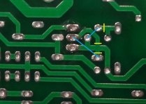
Here are the board changes that I think you need to make (please double-check!).
Yellow line denotes a trace cut. I'd recommend a Dremel with cutting disc if you have one.
Blue line denotes new wire link.
That should work. I was thinking about a slightly different route. Both will get the job done. Since the attachment for Q11 is wires, I may attach the base on top directly to the R13 lead and only need two trace cuts on the bottom.
Attachments
Terry, your way is even better. Great thinking. I suspect Struth meant to lay one of those two tracks on the topside.
Yeah, I'm not sure what happened there. The pin-out is wrong too. I'll get on it in the morning and see if that solves my problem. Right now I have a pretty big offset. Hopefully this will help with that too.
Hi Guys
Oop!
It seems there is a shorted trace from J11-B on the board.Pin-2 is shorted to pin-3. The fix is to slash the trace from pin-2 either side of where it crosses the trace from pin-3. Then add a wire link to join pin-2 to the end of R13.
Unmodified, the bias pot won't work and the amp will bias HOT - possibly destructive.
Eagle says the board and schematic are consistent. Must be bug that keeps it from seeing nets that are connected that shouldn't be... And then there's my bug...
When powering up, set the bias pot for maximum in-circuit resistance to set the output current to zero. The amp will usually pass a clean sine wave into no load and you have an initial verification that most things are working. Add a very light load and you should see some cross-over notch that can be dialled out using the bias pot.
R13 changes the range of the bias setting. Working againstR28 alone, the total bias voltage applied to the predriver bases is (R13/R28) x 650mV or so - the Vbe of Q11.
As the notes say, if you have a low-voltage split supply it is best to power up with that before going to the big supply.
Terry, you said: "The pin-out is wrong too". Pinout for what?
Have fun
Kevin O'Connor
Last edited:
Terry,
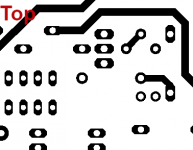
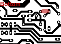
I was comparing your photo of the bottom copper to my copy of the PDF layout, and I noticed a difference. I've included the section from the bottom and top of the same region as your photo. The red highlights a trace that is not present in my copy of the PDF but is in your board. I downloaded my copy on 1/26. I've also included the same section from the top--perhaps you'll see some other difference there.
I was comparing your photo of the bottom copper to my copy of the PDF layout, and I noticed a difference. I've included the section from the bottom and top of the same region as your photo. The red highlights a trace that is not present in my copy of the PDF but is in your board. I downloaded my copy on 1/26. I've also included the same section from the top--perhaps you'll see some other difference there.
Attachments
C19 (22pF) does not appear to exist on these boards either, but the pads and traces are present on the PDF. So there are differences between the published PDFs and the Gerbers apparently.
Hi Guys
Oop!
It seems there is a shorted trace from J11-B on the board.Pin-2 is shorted to pin-3. The fix is to slash the trace from pin-2 either side of where it crosses the trace from pin-3. Then add a wire link to join pin-2 to the end of R13.
Unmodified, the bias pot won't work and the amp will bias HOT - possibly destructive.
Eagle says the board and schematic are consistent. Must be bug that keeps it from seeing nets that are connected that shouldn't be... And then there's my bug...
When powering up, set the bias pot for maximum in-circuit resistance to set the output current to zero. The amp will usually pass a clean sine wave into no load and you have an initial verification that most things are working. Add a very light load and you should see some cross-over notch that can be dialled out using the bias pot.
R13 changes the range of the bias setting. Working againstR28 alone, the total bias voltage applied to the predriver bases is (R13/R28) x 650mV or so - the Vbe of Q11.
As the notes say, if you have a low-voltage split supply it is best to power up with that before going to the big supply.
Terry, you said: "The pin-out is wrong too". Pinout for what?
Have fun
Kevin O'Connor
Hi Kevin, thanks for popping in. Perhaps "wrong" was not the right word to use. The "symbol" in the screen print is the same as used for all the other TO-22x transistors. Those all have either an ebc or bce pinout. This one is cbe or ebc depending on how you look at it. It confused me, that's all.
You say to cut the trace where the pin two crossed pin three and add a jumper. What about where the opposite side of the pot is shorted? Does it matter which side of the pot is shorted?
I am powering up with a lower voltage supply and through a light bulb tester with ad ammeter inline with the - rail. It actually powered up with low bias, 17mA.
Hi Jason and radio,
Good that you guys are watching in since you have these boards as well. I haven't looked for other things yet, I was just dealing with the first thing I found. I appreciate you guys helping problem solve. Hopefully by the time you build your boards we will have all the bugs worked out.
edit, How necessary is C19? I could figure a way to add it.
Blessings, Terry
Last edited:
Looks to me like Struth decided to use different compensation methods in combination, with C19 being some shunt (lag) compensation. I'd suggest we hear what Struth has to say about it since this is his baby. We can definitely add this capacitor P-P under board easily enough.
Looks like this wasn't built before being released into the wild...
Looks like this wasn't built before being released into the wild...
There is two-pole compensation formed using C8, C12 and R57. All the schematics I have seen have the shunt/lag compensation cap bypassing the VAS collector and emitter - not what C19 is doing here.
The fact that C19 is such a small value suggests to me that it can probably be omitted without any ill effects.
The fact that C19 is such a small value suggests to me that it can probably be omitted without any ill effects.
The C8, C12, R57 is what I recognize as TMC - Transitional Miller Compensation - and while it has two poles is a little different in function than normal two pole where R57 would be referenced to ground rather than the output rail. As for C19 it really doesn't matter where it terminates to, it provides frequency conscious loading to the VAS which I interpret as shunt (lag) compensation. The TMC is likely enough on its own but I'd like to hear from the circuits author anyway.
Hi Kevin, thanks for popping in. Perhaps "wrong" was not the right word to use. The "symbol" in the screen print is the same as used for all the other TO-22x transistors. Those all have either an ebc or bce pinout. This one is cbe or ebc depending on how you look at it. It confused me, that's all.
Terry, are you aware that the Vbe transistor is meant to be soldered to the little break out board (look at the perferated section on the bottom left of the PCB). That way the Vbe transistor can be screwed to the top of one of the output transistors for thermal tracking.
The traces on the break out board are such that the BCE pinout of a TO-220 cased
VBE is routed so that pin 1 = C; pin 2 = B; pin 3 = E. I wouldn't recommend soldering the VBE transistor directly to the main board as you'll experience thermal offset drift.
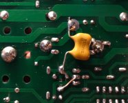
OK, I made the cuts and installed jumpers on one board. I turned the bias pot to full resistance. I brought the power up on a variac through a light bulb I stopped at +-50V rails. Bias 17mA, DC offset 1.2V. I began turning the pot and all of a sudden the bias jumped to 500ma light bulb shining brightly. The DC offset dropped to and 50mv. I shut off the power, waited for it to drain down and powered back on. Bias was at 17ma until the amp sat for about a 30-40 seconds and then the light went bright again and the bias shot up. I hooked up my scope and I see a jagged sinewave once the bias shoots up. I'm assuming it is oscillating. So I added the 22pf cap tot he bottom of the board but no change. I is possible I have something else wrong. I will begin the process of checking everything again. I have added a pic of the trace fix.
Blessings, Terry
Blessings, Terry
Attachments
Terry, are you aware that the Vbe transistor is meant to be soldered to the little break out board (look at the perferated section on the bottom left of the PCB). That way the Vbe transistor can be screwed to the top of one of the output transistors for thermal tracking.
The traces on the break out board are such that the BCE pinout of a TO-220 cased
VBE is routed so that pin 1 = C; pin 2 = B; pin 3 = E. I wouldn't recommend soldering the VBE transistor directly to the main board as you'll experience thermal offset drift.
Hi Ranchu,
I didn't notice that the little breakout board had the traces crossed.😱 Thanks for pointing that out. I didn't use the little board I just used wires. My bad.
Boy I really had my donkey ears on today. I found a couple solder bridges and fixed those. I hook everything back up expecting to see great things and still issues. Then I decide to start measuring everything and notice that I had never installed C16. What a dope. Anyway, no more anything until I procure a couple of those, Sheesh!
Eagle says the board and schematic are consistent. Must be bug that keeps it from seeing nets that are connected that shouldn't be...
Hi Struth,
If I understand what you are saying correctly......
I don't think there is an Eagle bug. Traces that overlap, are too close to one another or too close to the edge of the board etc, are picked up when you run Tools > DRC (design rule check). If you are not regularly doing a DRC then you may be in for a shock!
When Eagle says the Board and Schematic are consistent, it only means they are in-sync so backward and forward annotation will work.
regards
With that said, I guess I will be going through the board with the schematic and looking through each trace and circuit. I have problems so I need to find where it is failing. This has been a rough week. I fired up an nx amp and it has issues too. Fun stuff!
Blessings, Terry
Blessings, Terry
- Status
- Not open for further replies.
- Home
- Amplifiers
- Solid State
- 250w 8ohm amplifier