Edit.
Ahh, j11a matches j11b.
The Vbe multiplier is missing.
The current through the resistor string does not account for the 6mA going from CCS to VAS. Some of it is going through the missing multiplier.
Check the voltages across the multiplier and especially check their polarities. Vce, Vbe, Vcb
Could you remove the NFB cap and check/measure it's leakage at half maximum voltage?
It may be that you did not reform this electrolytic and it is drawing excessive leakage through the feedback loop.
Last edited:
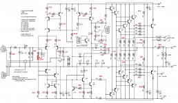
What do you mean the multiplier is missing? isn't that Q11? It is right in the middle of the schematic. I did see that I didn't list the voltage drop across the trim pot. It is .435V. I added it to the attached schematic.
Which is the NFB cap and how do I measure it for leakage?
I did not "reform" any caps, but the whole system was brought up slowly on a variac and driven through a light bulb for the first few hours of testing.
Thanks, Terry
EDIT; I am attaching a schematic with voltages for the VBE as well. I noticed I hadn't shown them on the first one.
Attachments
Last edited:
My edit states "ahh".
I saw that the Vbe is on the schematic.
remove the capacitor.
Attach a 10k resistor. Use 9v to charge the cap through the resistor. after a few minutes the cap should be near it's final voltage. Measure the Vdrop across the resistor. That will tell you the total current passing through the resistor.
Some will be charging current and some will be leakage current.
after just 10seconds of charging the charging current is still quite high and will swamp the leakage current. Even though the leakage is worse before slow charging commences.
After a minute the charging current and the leakage current will possibly be similar.
After 5minutes the (still reducing) leakage current should be larger than the charging current. That's the current that may give a clue.
Leave the cap charging/leaking for 12 hours and remeasure the leakage current.
Take it off charge and let is slowly leak away for another 12hours. Discharge it with a 1k resistor.
Recharge through the 10k resistor for 12 hours. remeasure the leakage current. The leakage after two 12hour spells, may now be so low that you cannot measure a Vdrop across the 10k.
Change that to 100k (or even 1M0). And charge for a further hour. Measure the leakage current.
Each slow recharge is gradually reducing the leakage current. You have reformed the capacitor.
I have suggested numerous times on this Forum that all electrolytics be reformed before putting them to use. This removes misbehaving caps from the debugging strategy. This process also removes the "burning in time period" that is mistaken for in circuit reforming that takes nearly for ever to do at the very low voltages across some of the electrolytics. eg. the NFB cap should, if the amp is behaving properly, have 10mVdc to 100mVdc across it. It never really properly reforms in circuit.
Last edited:
Hi Andrew,
We were typing at the same time. Please have a look at the schematics I attached and see if that helps identify the problem. It was a little difficult to nail down the voltages in the multiplier because toughing the test points with the probe would cause the bias to change and thereby the voltages. Also, as the amp warms up the voltages at the multiplier were gradually dropping. I tried to just pick a point in time and quickly take the measurements.
Also, You didn't answer the question. Which one is the "NFB" cap?
Would it still help if I disable D6 & D7?
Thanks, Terry
The NFB is the group of components: R16, R15, C4
C4 is the NFB capacitor. It blocks DC and forms a high pass filter inside the amplifier circuit.
For best performance this capacitor should have negligible AC voltage and negligible DC voltage across it. If you remove the 4 protection diodes I think you will fine that it will have enormous DC voltage. That is the symptom we are trying to eliminate.
The compensation components are C11, R36? R57?, C19, C12, C6?, C7, R49,
There's something wrong around the Vbe resistor string, The transistor voltages don't match the resistor voltages. Is there continuity in the connections?
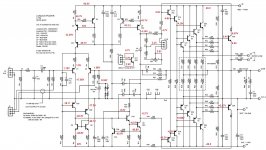
That is probably my fault. I just added the voltages from the vbe this morning. It is likely that the rest of them were taken a couple of days ago and it is possible that the variac was set slightly different. I will sit back down and let the amp warm up for a while and then take all the measurements again. Like I said, the voltages change as the amp warms up.
Thanks, Terry
Thanks, Terry
OK, I took some better measurements. I plugged straight into the wall with a 50V supply. No variac, no light bulb. Attached is the schematic.
Thanks, Terry
Thanks, Terry
Attachments
Last edited:
No need to apologize, thanks for helping. Yes it was a typo, I fixed it. Please feel free to help all you can. I am trying to figure out if I have made a mistake somewhere ore if there is a problem with the PCB.
Thanks, Terry
Thanks, Terry
Hi Ranchi,
I am using MJE340/350. I have the orientation reversed from the silk screen per Kevin's instructions.
Sorry terry please disregard my post!
Last edited:
9.75Vdc across the protecting diodes. Have these blown due to excessive offset?
Note that the VAS & Q8 & Q14 & Q16 Vbe has dropped to just <=0.4Vbe. They are just about turned off.
Q3 has 0.8Vbe. It is turned on HARD. Q23 is turned on even harder.
The Vbe voltages tell you that something is not working.
The resistor currents should give a clue to where the errors may be.
Pin1 of J11b is still very unmatched to the two voltages on the other side of pin1 of j11a.
There are now so many big voltage errors, that I think you may have blown something with a slipped probe.
Last edited:
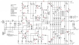
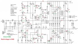
Took measurements for VBE of all transistors and added them to the schematic in green text. Q8 & Q10 looked suspicious so I replace them. No change. Replaced the protection diodes, no change.
Please see attached.
Someone please help me understand where the 9.34V comes from at the protection diodes when one side is R15 with 1.5V and the other is ground?
Thanks, Terry
Please see attached.
Someone please help me understand where the 9.34V comes from at the protection diodes when one side is R15 with 1.5V and the other is ground?
Thanks, Terry
Attachments
Last edited:
did you check the board and confirm that it agrees with your schematics?
the 3.57 volts offset tells us that the negative side of the ckt is not working as it should..
the 3.57 volts offset tells us that the negative side of the ckt is not working as it should..
Hi Tony,
Yes, I used a highlighter on a schematic and traced every circuit. The only deviation I found was the troubles with the traces at the VBE multiplier and trimpot that have been noted earlier. I believe I have corrected that and now all traces agree with the schematic.
I agree, the negative side is not working properly but I can't see why. Q10 & 12 have almost no VBE at all. I replaced both with no improvement. Q14 &16 have very low VBE so I replaced those with no improvement. I don't want to just keep replacing parts willy nilly. I will soon run out of parts and the boards take a beating. Any help is welcome.
Thanks, Terry
Q8,10,12 and associated circuits needs to be checked, could be wrong valued resistor,
sometimes the color coding could be different from actual readings...
sometimes the color coding could be different from actual readings...
The resistors were not installed by color coding. I measured them. I have triple checked them at this point. Could it be that one of the called out values is wrong?
could it be you installed the wrong resistor in the wrong hole?
you do not need Q12 as yet, you can pull it out of the board in the meantime
and see what gives, that trannie limits base current to VAS in case of overloads...
when everything is normal, you can put it back, same with the Q25, Q26
you can take them out in the meantime and focus on the offset problem...
the new voltages do not agree with what was presented earlier.
Have you changed something else?
Or has the amplifier settled into a different state?
Check again for oscillation, while you are taking your measurements. i.e. does the amp oscillate while your DMM probes are touching the test points?
Have you changed something else?
Or has the amplifier settled into a different state?
Check again for oscillation, while you are taking your measurements. i.e. does the amp oscillate while your DMM probes are touching the test points?
- Status
- Not open for further replies.
- Home
- Amplifiers
- Solid State
- 250w 8ohm amplifier