The open-loop PSRR to the negative rail is essentially zero. This is because R7's local feedback around the voltage amplifier is referenced to the negative rail. The 35dB of global feedback improves the closed-loop PSRR to 35dB, which is why I expect the amplifier to hum.
Your version has higher loop gain (45dB).
The solution is to get rid of R7. Instead, load the voltage amplifier with a resistor to ground.
Ed
Your version has higher loop gain (45dB).
The solution is to get rid of R7. Instead, load the voltage amplifier with a resistor to ground.
Ed
C6/C7 can be better for stability since there is less inductance to the output transistor collectors, or at least can be depending on layout.
The effect of R8/C2 highly depends on the source impedance and feedback network impedance, which is curiously absent from the schematic.
It clearly works, but it could be made safer by adding an input capacitor and a more reliable bias generator, and at least some simple protection.
I think a better goal than indiscriminately improving performance would be to make a design with less transistors that is as good or better. That should be possible and might be something people would actually build.
C6=C7 = 100nF MKS3C6/C7 can be better for stability since there is less inductance to the output transistor collectors, or at least can be depending on layout.
can be combined into a single capacitor to GND.
R18||C11, R19||C12 & R20||C13, R21||C14The effect of R8/C2 highly depends on the source impedance and feedback network impedance, which is curiously absent from the schematic.
on the right of the sheet you can clearly see the missing network!
X3 is the amplifier output node!
When I open my eyes, I see the ac-coupling and also a very rudimentary limiter formed by K8 (or Q8).It clearly works, but it could be made safer by adding an input capacitor and a more reliable bias generator, and at least some simple protection.
You could do that, but that is not the purpose of this thread.I think a better goal than indiscriminately improving performance would be to make a design with less transistors that is as good or better. That should be possible and might be something people would actually build.
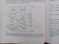
I present this circuit for general discussion, it is based on the ETI project 470 from November 1979. My scaling to 20 watts (into 8 ohms) works and has worked flawlessly for several years.
Fire away!
"The effect of R8/C2 highly depends on the source impedance and feedback network impedance, (...)" [keantoken]
@keantoken
Then please start a reflective analysis once again.
thx and kindly,
HBt.
hbtaudio - Take the negative rail ripple voltage, reduce it by 45dB, and this is what you should see at the output.
Ed
Ed
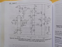
Consequently, we are replacing the TIP142/147 Darlington with the classic EF2.
But now we have to be very careful that the 20WPA doesn't mutate into Douglas Self's BLAMELESS amplifier.
greetings,
HBt.
🧙♂️
A (differential + CCS) + (enhanced VAS + CCS) + (4 x BDV64/65) would do a much better job even if there s no current mirror
for the IPS, this ETI design is flawed from the start and trying to compensate its shortcomings is just to give to the pig some
lipstick, btw Self s so called Blameless is basicaly a discrete and simplified uA741.
May I kindly repeat myself:Obviously the TO is immune to advice.
This thread is for the objective, i.e. qualified, analysis of the present circuit (it is based on the ETI 470 project) - gladly unsparingly and freely from the liver, as long as statements or findings are qualified.
Interjections such as the typical interjections from you Bucks Bunny, serve another well-known purpose and have absolutely nothing to do with the matter at hand.
This is certainly not about giving advice or being a know-it-all. If I were immune, I would obviously not be the person I am.
Dear BB,
please participate in my organized discussions as one would expect from a German physics graduate and established pensioner - you call yourself an expert, so please contribute to a friendly and cultivated discussion culture with your expert knowledge.
Many thanks and best regards,
HBt.
PS
You are welcome to contact me at any time by PM, e-mail or telephone.
You're absolutely right, that's the basic principle or concept. I have attached two photographs for direct comparison.(...) this ETI design is flawed from the start and trying to compensate its shortcomings is just to give to the pig some
lipstick, btw Self s so called Blameless is basicaly a discrete and simplified uA741.
Attachments
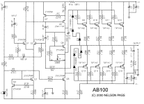
Here we are now talking about a topology that corresponds almost 1 to 1 to that of the “AB100 by Nelson Pass”, but also follows the general recommendation of Douglas Self ..!A (differential + CCS) + (enhanced VAS + CCS) + (4 x BDV64/65) would do a much better job even if there s no current mirror
for the IPS, (...)
The initial (OPS) duo becomes an initial (OPS) quartet with the BDV64B & BDV65B (n=4 parallel) Dalington BJTs ..!
Attachments
In order to better understand this,hbtaudio - Take the negative rail ripple voltage, reduce it by 45dB, and this is what you should see at the output.
Ed
I calculate the worst case and compare the following:
- P= 20W continuous tone at RL=8Ohm with my PSU
- leads to an additional unwanted power (negative hum) of just under 10µW at the output
- 10 * log_10[10µW/20W] = -63dB!
I hope this undisputed point is now off the table.
Last edited:
How do we explain the huge gap between the values given by the authors of the original article and the deduction that can be read here?
Did Trevor & Phil lie?
"SNR better then -110dB at full scale"
Did Trevor & Phil lie?
"SNR better then -110dB at full scale"
Here we are now talking about a topology that corresponds almost 1 to 1 to that of the “AB100 by Nelson Pass”, but also follows the general recommendation of Douglas Self ..!
The initial (OPS) duo becomes an initial (OPS) quartet with the BDV64B & BDV65B (n=4 parallel) Dalington BJTs ..!
ETI used the same topology as Pass, the difference is that they used a huge current for the IPS and their botched VAS.
Only thing lacking in both case is a buffer for the VAS.
It s incredible how much a single BC546 addition can improve this topology, even without a current mirror it still improve THD by something like 20dB, this has to be the most cost effective enhancement ever.
As for ETI s optimistic numbers i m about sure that they used a regulated PSU for their tests, this way all they measured was
the amp s white noise, at 22V RMS output signal as reference this amount to 65uV output noise, wich is about in line with
their amp s relatively high gain of 33.5dB, this put the input noise at 1.37uV or 9.25nV/sqrt(Hz) wich is easily achivable with
an IPS using BC transistors.

We are mixing PSRR and S/N, but the results are consistent.
A ripple of 10uW into 8 ohms is 9mV RMS at the output. Adding 45dB of PSRR, the ripple on the negative rail would be 1.6V RMS. That is reasonable.
Millivolts of ripple at the output are poor for a solid-state amplifier. Compare the S/N against figure 3 in Stereophile's measurements of poor, average, and good amplifiers.
I think that the authors simply goofed in their calculated S/N.
Ed
Let's stay with the power supply for a moment, especially the ripple
Let's assume a charging capacity of 10mF.
In my simplest calculation from posting #131, I deliberately ignore the resulting time function, which leads to a much larger effective (RMS) voltage value than it actually occurs.
To illustrate this, I now offer a corrected, approximate value. The correction factor now introduced (of 0.191) leads to a much more realistic value for U_ripple_rms.
Of course we can approximate numerically even further, but what's the point - I just want to make it clear that the pure amplifier circuit forms a unit with the power supply.
With the more correct rollover, I suddenly end up with -74.43dB !
#
The power supply I use consists of:
3*4700µF -> 0,47Ohm -> 3*4700µF
and
3*4700µF -> 0,47Ohm -> 3*4700µF
PI configuration; i.e. charging and smoothing included, so I can push the criticized PSRR aside without any stomach ache. With this power supply, the following is now calculated (again, with a quite good approximation):
better -89.42dB !
Everything depends on the power supply unit.
☕
Last edited:
full agreement!
Unfortunately, even I (as the operator of an MF-A1) have to admit without hesitation that from a technical point of view (and this is what this thread is about) an A1 is a poor construct, especially if we take objective measurements into account.
From a Burmester product I expect (in return) absolutely impeccable measured values.
I also assume that fact.I think that the authors simply goofed in their calculated S/N.
But the ultimately decisive question is:
Could the ETI 470 proposal achieve its goal? Namely, low distortion and, above all, lowest IM. A direct comparison with the well-known Lohstroh-Otala amplifier proposal makes our eyes pop out.
ETI used the same topology as Pass, the difference is that they used a huge current for the IPS and their botched VAS.
Only thing lacking in both case is a buffer for the VAS.
Isn't this form of voltage amplifying stage (in Douglas Self's diction: VAS) supposed to be the gimmick, i.e. the bungling the special feature?
What is absolutely correct and quite incidental is not the fact that we thereby free the IPS (here we form the well-known and so important difference) from any load ..!It s incredible how much a single BC546 addition can improve this topology, even without a current mirror it still improve THD by something like 20dB, this has to be the most cost effective enhancement ever.
Compared to the standard circuit chosen by Nelson Pass, an indication of his elephants in the room would now be honorable:
AB100 vs. ETI 470 (or the 20WPA interpretation)
+1As for ETI s optimistic numbers i m about sure that they used a regulated PSU for their tests, this way all they measured was
the amp s white noise, at 22V RMS output signal as reference this amount to 65uV output noise, wich is about in line with
their amp s relatively high gain of 33.5dB, this put the input noise at 1.37uV or 9.25nV/sqrt(Hz) wich is easily achivable with
an IPS using BC transistors.
greetings,
HBt.

hbtaudio - Take the negative rail ripple voltage, reduce it by 45dB, and this is what you should see at the output.
Ed
What reduction can we expect in dB compared to the "45dB" of the 20WPA with the AB100? And above all, why?
Attachments
A bipolar transistor is a differential amplifier. The base is the inverting input and the emitter is the non-inverting input. A feedback resistor between the collector and base is fine only when the emitter is at ground potential.
Amplifiers (other than the ETI) achieve high PSRR because the collector current does not vary much with collector-emitter voltage.
Ed
Amplifiers (other than the ETI) achieve high PSRR because the collector current does not vary much with collector-emitter voltage.
Ed
More accurately, the lower the amp s PSRR the more everything depends on the PSU.Everything depends on the power supply unit.
☕
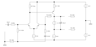
View attachment 1369984
Isn't this form of voltage amplifying stage (in Douglas Self's diction: VAS) supposed to be the gimmick, i.e. the bungling the special feature?
In this form that s a voltage amplifier, but not in the case of Self amp, on your schematic the collector load define
the gain along with the emitter load while in the case of our discrete 741 the gain is defined by the IPS loading and the
VAS input and output impedances, that s why the addition of this transistor, TR12 in Self s schematic, is so beneficial
as it decrease the IPS loading all while increasing the VAS input and output impedances and hence the IPS and VAS gains.
- Home
- Amplifiers
- Solid State
- 20WPA