this is a comment on the schema that was in the attachment. can repeat once again looking at that attachment.You did not say that in post 1,612, not clearly at least.
, but it’s not logical to parallel the driver for mosfets. in this case, the driver stage distortions add up because there is no additional reduction in output resistance to drive the mosfet gates.
why different beta? everything is equalized by additional emitter resistors, and more current allows the driver to be in linear mode at twice the current swing.Paralleling driver transistor with different beta, is this goos idea?
and what is that supposed to mean? questions of the nuances of circuitry are not available to everyone, simply because you don’t have to delve so deeply, it’s not always possible to determine by ear ...This amp is on the web quite long time and nobody said what you say here.
of course it is worth checking in the model, I had a similar option and it was rejected by me for the above reasons.I will simulate it, could you point to what to take attention?
This statement, i can't catch the meaning.... the driver stage distortions add up because there is no additional reduction in output resistance to drive the mosfet gates.
Yes, the more current and lower output impedance the driver works with, the better the mosfet is controlled.This statement
do you think otherwise?
I don't understand the meaning either. you can help?i can't catch the meaning.
why separate drivers for each pair of mosfets? next to the topic there is a similar solution - how is this justified?
Sure that, but how does this relate to the attached example?Yes, the more current and lower output impedance the driver works with, the better the mosfet is controlled.
if you divide the driver for each pair of mosfets, will the driver current decrease?Sure that, but how does this relate to the attached example?
The MOSFETs present capacitive load. Drivers simply charges and discharges parasitic gate capacitance. Emitter resistance influence charge/discharge time.I don't understand the meaning either. you can help?
why separate drivers for each pair of mosfets? next to the topic there is a similar solution - how is this justified?
But,
if it charges two MOSFETs with one driver or four MOSFETs with two drivers it is all the same.
What we get in parallel configuration is additional emitter resistance to equalize the currents, therefore slowing the circuit what the constructor tend to avoid.
is that what you ask? or do you approve? It seems that the width of driver' working area is not important to you.But,
if it charges two MOSFETs with one driver or four MOSFETs with two drivers it is all the same.
What we get in parallel configuration is additional emitter resistance to equalize the currents, therefore slowing the circuit what the constructor tend to avoid.
the author said that he would model and tell the result ....
It's better to wait than jump to conclusions.
P.S. I made my conclusions, and I'm not going to design such nonsense ....except for the case when the value of the output power is more important than the quality.
Last edited:
It is really simple math, no need for modeling. Two MOSFETs cca 2nF, one driver Re (suppose 10mA question current) cca. 2.6 - 3R.
Four MOSFETs 4nF, two drivers parallel cca. 1.3 - 1.5R.
Time constant = R*C
Count yourself.
Four MOSFETs 4nF, two drivers parallel cca. 1.3 - 1.5R.
Time constant = R*C
Count yourself.
Well, now i'm sorry to ask, that driver's working area, could you explain?It seems that the width of the driver's working area is not important to you.
It is widely assumed that the value of the input capacitance given in the mosfets description corresponds to the input capacitance that is actually used in the designs, many designers subsequently fell into this trap.It is really simple math
waiting for simulation results...
think for yourself...
It doesn't change anything about the problem we are discussing right now.It is widely assumed that the value of the input capacitance given in the mosfets description corresponds to the input capacitance that is actually used in the designs, many designers subsequently fell into this trap.
waiting for simulation results...
think for yourself...
Google translator difficulties, it looked like this:Well, now i'm sorry to ask, that driver's working area, could you explain?
"You don't seem to care about the linear operating range of the mosfet driver."
if you are correct, then you don't have to bother with the discussion...It doesn*t change anything about the problem we are discussing right now.

Hi Damir sorry for the slow response I have that latest board revision 1.3.2b ... you posted you had some more available I have 6 of them and plan to used them with a balanced preamp. Though could use suggestion if I should build the balanced version or use a balanced to single ended buffer instead.
Do you have small additional balance board like in photp?Hi Damir sorry for the slow response I have that latest board revision 1.3.2b ... you posted you had some more available I have 6 of them and plan to used them with a balanced preamp. Though could use suggestion if I should build the balanced version or use a balanced to single ended buffer instead.
Adding a balanced to single ended buffer instead is solution too, but it will degrade the amp in some way.
The link for balance version: https://www.diyaudio.com/community/threads/200w-mosfet-cfa-amp.243481/page-71#post-5725721
BR Damir
Attachments


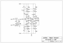
Nope I don't have those, I have the amp boards and voltage reg board along with a small board for multiple resistors.
Unfortunately I don't have any spare.Nope I don't have those, I have the amp boards and voltage reg board along with a small board for multiple resistors.
If you are willing to share with a US based board house I'd get some built. how many 1.3.2b boards do you have left BTW if any ?
- Home
- Amplifiers
- Solid State
- 200W MOSFET CFA amp