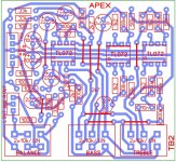
For who want here is the pcb for TB1 not so professional this is my first pcb copy. If i do any mistake please corect me.
![IMGDEAD]](/community/proxy.php?image=http%3A%2F%2F%5BIMGDEAD%5Dhttp%3A%2F%2Fi66.tinypic.com%2Ffa8l1y.jpg%5B%2FIMGDEAD%5D&hash=5768552e739226614e0250934ff94ea9)
Sprint file: https://mega.nz/fm/s6ITCDQa
Sprint file: https://mega.nz/fm/s6ITCDQa
For who want here is the pcb for TB1 not so professional this is my first pcb copy. If i do any mistake please corect me.
Sprint file: https://mega.nz/fm/s6ITCDQa
On TL072 pin 1 is not connected...
On TL072 pin 1 is not connected...
Thank you sir I will corect that.
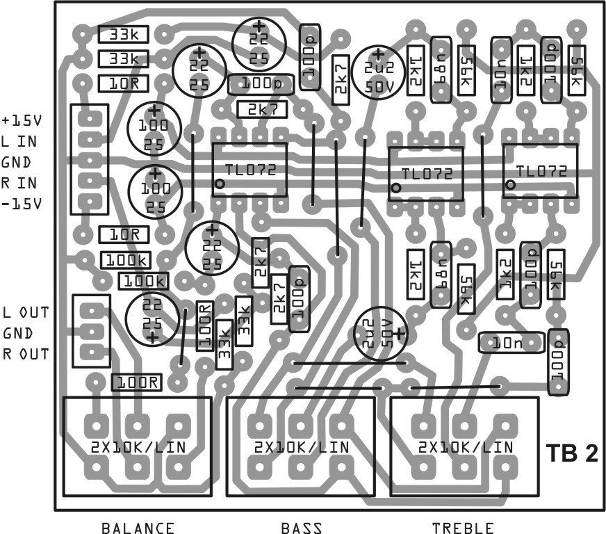
Sir do you have the pcb for TB2
Use this TB2 pcb design.
Attachments

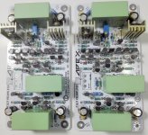
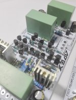
P30ZF
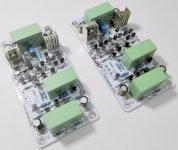
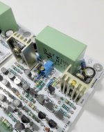
P30ZF preamplifier ...... ready for testing !
Regards,Alex
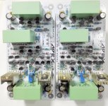
P30ZF preamplifier ...... ready for testing !
Regards,Alex
Attachments
-
 IMG_20170417_184811-001.jpg984.1 KB · Views: 1,725
 -
 IMG_20170417_184831-001.jpg560 KB · Views: 985
 -
 IMG_20170417_184854-001.jpg525.7 KB · Views: 771
 -
 IMG_20170417_184910-001.jpg477.4 KB · Views: 331
 -
 IMG_20170417_185057-001.jpg928.7 KB · Views: 364
 -
 IMG_20170417_185235-001.jpg798.7 KB · Views: 372
 -
 IMG_20170417_185253-001.jpg664.1 KB · Views: 436
P30ZF preamplifier ...... ready for testing !
Regards,Alex
Nice work!
Let us know how it sounds!
Thanks
Do
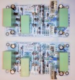
P30ZF preamplifier ...... ready for testing !
Regards,Alex
Nice work, olaf test P20 with same zero feedback topology and this will be first P30ZF test.
Regards
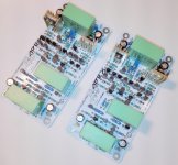
P30ZF preamplifier ...... ready for testing !
Regards,Alex
Dear Alex,
Can you kindly post the schematics also?
--gannaji.

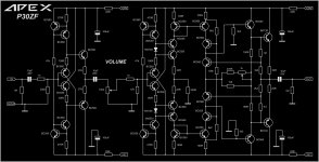
Schematic P30ZF
Schematic right here 😉
Dear Alex,
Can you kindly post the schematics also?
--gannaji.
Schematic right here 😉
Attachments
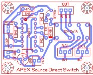
Use this TB2 pcb design.
I made TB-2 layout (Apex clone) in sprint in case anyone wants it. checked it, its fine.
Attachments
Last edited:
I made TB-2 layout (Apex clone) in sprint in case anyone wants it. checked it, its fine.
Thank you Prasi you save me. I work two days on that pcb but nothig good. I don`t have so much talent. You pcb looks great.
Do you can make a copy of these pcb`s if you have some time free?
Thanks in advance!
An externally hosted image should be here but it was not working when we last tested it.
An externally hosted image should be here but it was not working when we last tested it.
Thank you Prasi you save me. I work two days on that pcb but nothig good. I don`t have so much talent. You pcb looks great.
Do you can make a copy of these pcb`s if you have some time free?
Thanks in advance!
Its very easy to make clone in sprint. Go to extras-Scanned Copy.
Then select the image of the PCB.
Then simply make tracks on appropriate layer (silk on S1, copper on C2, outline on O, etc)
I have attached, both TB2 and source direct switch. you can make TB1 following above procedure.
reg
Prasi
Attachments
Last edited:
Its very easy to make clone in sprint. Go to extras-Scanned Copy.
Then select the image of the PCB.
Then simply make tracks on appropriate layer (silk on S1, copper on C2, outline on O, etc)
I have attached, both TB2 and source direct switch. you can make TB1 following above procedure.
reg
Prasi
Thank you very much Prasi. I will try. Have a nice day!🙂
Thank you very much Prasi. I will try. Have a nice day!🙂
Learn to catch the fish, man!; you will never go hungry again.
just a little saying.
all the best. If you need any help, pl ask.
Prasi
edit: you can utilize Apex footprint of components (resistors. capacitors, IC's, connectors, etc ) from the TB-2 and SDS file I shared above. Just select all silk tracks/pads related to a particular component using (shift key) and save them as appropriate component. Your work will be much easier.
Last edited:
I hate sprint!, never will use it for making new design! you can join any pad with any pad..how stupid can it be! I dont know how Alexmm and Sonal Kunal manage, but its not a good software for making pcb design. lots of scope for mistake... pl spend some time and learn eagle/some other schematic capturing software (that Jwilhelm/ Valery use). You will have exact reproduction of schematic.
But one and most important advantage with sprint is, anyone can start cloning and designing pcb in literally no time!!!!
But one and most important advantage with sprint is, anyone can start cloning and designing pcb in literally no time!!!!
Dear sir,
I agree with you.
Te resistor pads are very small in eable, how do we change the default size and shape of pads?
I agree with you.
Te resistor pads are very small in eable, how do we change the default size and shape of pads?
I hate sprint!, never will use it for making new design! you can join any pad with any pad..how stupid can it be! I dont know how Alexmm and Sonal Kunal manage, but its not a good software for making pcb design. lots of scope for mistake... pl spend some time and learn eagle/some other schematic capturing software (that Jwilhelm/ Valery use). You will have exact reproduction of schematic.
But one and most important advantage with sprint is, anyone can start cloning and designing pcb in literally no time!!!!
- Home
- Amplifiers
- Solid State
- 100W Ultimate Fidelity Amplifier