I find it impressive how you guys handle all these curcuits and boards
me, Im a simple guy with a simple mind 😛
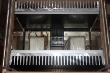
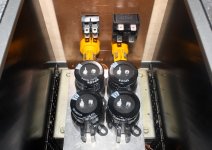
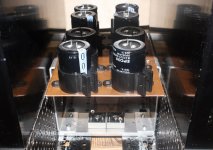
'back' and 'front' mounted, and ready for the connectors
and sidewiev of inside layout
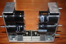
supply caps will carry the main amp board
(in total,12x 5600uf/100V/6A, 35x45mm)
me, Im a simple guy with a simple mind 😛
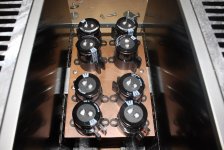
'back' and 'front' mounted, and ready for the connectors
and sidewiev of inside layout
supply caps will carry the main amp board
(in total,12x 5600uf/100V/6A, 35x45mm)
Attachments

Tin,
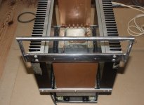
can you turn the PCB+Output Devices upside down?
The sinks will dissipate more heat, or run the Output Devices cooler if you can get the Outputs lower down.
can you turn the PCB+Output Devices upside down?
The sinks will dissipate more heat, or run the Output Devices cooler if you can get the Outputs lower down.
The sinks will dissipate more heat, or run the Output Devices cooler if you can get the Outputs lower down.
yes, I know
output will be mounted just below middle of the 200mm heatsink (height)
remember, trafos are actually below the heatsinks 😉
supply caps carrying the main board basicly stand on top of the trafos
and caps are 45mm
I want easy access to mounting screws on output devices
and I need to do some hardwire mounting on outputs
I just have to put my faith in those big heatsinks
and that the convection system actually works
and hey, remember, both heatsink are for one mono channel
(NPN on one heatsink, and PNP on the opposite)
edit, since my sidewiev could appear confusing, I have attached a smaller drawing, showing heatsink also
Attachments

read Cordell.
He suggests that N & P should not be separated.
He goes further, suggesting alternating N&P, such that the N to P leads are very close together for more effective canceling of radiated fields.
He suggests that N & P should not be separated.
He goes further, suggesting alternating N&P, such that the N to P leads are very close together for more effective canceling of radiated fields.
well....that depends on a number of things
the way I do it, the devices are not more seperated more than in any other designs of this size, if you look at the whole picture, from one end to the other
largest distance from ANY component to middle of amp will be about 100mm
its basicly like one big IC 😀
the way I do it, the devices are not more seperated more than in any other designs of this size, if you look at the whole picture, from one end to the other
largest distance from ANY component to middle of amp will be about 100mm
its basicly like one big IC 😀
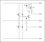
Overload current detect can be add to any amp to activate PRO input on NE555 protect.
how its fit to any amp with diferrent supply and output transistor type.....any advice for the value of component that not present on the schematic?
best regard,
read Cordell.
He suggests that N & P should not be separated.
He goes further, suggesting alternating N&P, such that the N to P leads are very close together for more effective canceling of radiated fields.
i am more of a Leach fan, followed their debate in the
Audio magazine years ago...😉
none that i can remember, but i tend to follow what people do, not what they say...
Leach amps were built by diy'ers all around the world, including me and these amps work...
Leach amps were built by diy'ers all around the world, including me and these amps work...
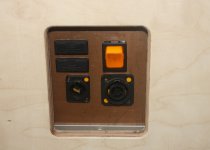
thinking about a input mute switch
and signal selector switch with two input options
one straight/bypass, and one with attenuation
maybe a LDR att
but not sure it would make sense
maybe just a 5 step 'att switch'
and signal selector switch with two input options
one straight/bypass, and one with attenuation
maybe a LDR att
but not sure it would make sense
maybe just a 5 step 'att switch'
- Home
- Amplifiers
- Solid State
- 1000W Simple PA Amplifier