Good luck all. I opened a spot for the guide and build of the Pass N Channel VFET.
I look forward to seeing the build come together...
GL
JT
I look forward to seeing the build come together...
GL
JT
Most of the general assembly of the VFET pt 1 will carry over well to pt 2. In particular, pay attention to the location of the OS brackets – they are best positioned toward the front (thick plate) of the amp, in order to leave sufficient room for the various FE boards.
Nelson's document is a good guide for populating the boards with their components. The overall wiring diagram in that document should be followed closely as well. What remains tbd is the location of the new PS filter board and the wire lengths. These you may solve as a community of enthusiastic (even fearless) amp builders. 😉
Nelson's document is a good guide for populating the boards with their components. The overall wiring diagram in that document should be followed closely as well. What remains tbd is the location of the new PS filter board and the wire lengths. These you may solve as a community of enthusiastic (even fearless) amp builders. 😉
Actually, being a larger board may mean less problems with the cables, and I’m sure they have added a couple extra inches to the cables already! 🙂
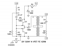
Latest PDF and Schematic from Papa... Updated 08/06/21
https://www.diyaudio.com/forums/attachment.php?attachmentid=972593&d=1628282682
https://www.diyaudio.com/forums/attachment.php?attachmentid=972593&d=1628282682
Last edited:
I’m standing by with slober & wire!
I believe you may find 63/37 lead-tin solder more effective. 😉
Last edited:
Also take note about the switch discussion in the build thread, should be a double pole type, but it seems a single pole was supplied in the kit according to members who are lucky enough to have received theirs. Also the switch is not mentioned in the BOM as part of the build guide.
also it looks like there still may be a thing or two that will need to be changed...
Ben posted this: https://www.diyaudio.com/forums/att...2606d1628286248-diy-sony-vfet-pt-1-a-2-ps-jpg
Ben posted this: https://www.diyaudio.com/forums/att...2606d1628286248-diy-sony-vfet-pt-1-a-2-ps-jpg
also it looks like there still may be a thing or two that will need to be changed...
Ben posted this: https://www.diyaudio.com/forums/att...2606d1628286248-diy-sony-vfet-pt-1-a-2-ps-jpg
Only in the schematic of the psu if I think. The board is ok.
On another note, I have some 82ohms instead of 100ohms included in the kit for R4 of the OS board. They are only gate stopper to prevent oscillation if I understand correctly so they should be ok but I would like to confirm with someone more knowledgeable than me before soldering them in.
Attachments

you;re good with anything between 47 and 220R
Great thank you ZM!
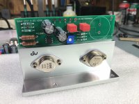
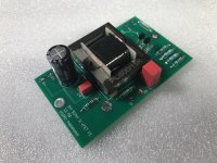
The boards are looking great! Everything is already stuffed appart from the big caps on the output which will be upgraded with some Nichicon KG, and C2 on the front end which will be replace with some Nichicon KZ. And I have to say that I really like the nice finishing touch from the master 😀
Attachments
the input 1k R1 is only for protect the jfet ?you;re good with anything between 47 and 220R
ie can be remove at risk ?
Attachments
Great thank you ZM!
The boards are looking great! Everything is already stuffed appart from the big caps on the output which will be upgraded with some Nichicon KG, and C2 on the front end which will be replace with some Nichicon KZ. And I have to say that I really like the nice finishing touch from the master 😀
Very nice! I wish I could say I'm not jelous, but I'd be a LAD if I denied it. 😀
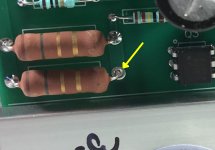
@Ylab
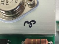
Is this solder joint your work? It cannot be from Papa, isn't it?
Ahah thank you for spotting that! No it’s not my work but I should have seen this 😱
Last edited:
I can bet it looks proper from bottom side
Yes everything looks great bottom side. I’ve just reflowed everything and it look great top and bottom
- Home
- Amplifiers
- Pass Labs
- DIY Sony VFET pt 2 (N-Channel Build)