You get the values of the caps from this schematic? C4 is 4p7 increasing to 220uF seems a lot. what values you suggest for C13? what will be the impact soundwise?The value of the capacitor in question is best chosen by ear because it's so instructive to hear the differences and get a feel for the design. Anyhow, with the transistor I used and the layout I used I found that a value around 47pF would be a good starting point. I found that 15pF was too small (sound was not quite right, a little bright or something) and 100pF is too big (sound loses it's magic whatever that means).
In your schematic, I would advise using high quality electrolytic (e.g. Nichicon MUSE or whatever they call their hi end audio range these days) for C4 and C13. The capacitor that filters the power to the LTP (C13) can be interesting to try different values. The bootstrap cap, C4, can be increased to 220uF if a high quality cap is on-hand as it supports lower frequencies better.
The input cap, C6, is usually a high quality film type and needs good space for the higher quality ones. However, many years later I discovered that I got great sound from using a Nichicon Bi-Polar (audio grade) capacitor of around 10uF but this does change the time constant at the input.
It's a great amp to DIY.
for C6 I have a WIMA or KEMET PP.
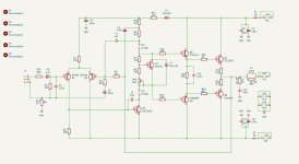
Attachments
I have an Aliexpress one LLC https://www.aliexpress.com/item/100...order_list.order_list_main.437.d401180252YHLXyes could be... its still R2 in line. so as i wrote...i do not check all the posts.
normally a current of 1mA each transitor is good so i guess 2mA total(for both)
is rated 700W but it is an 350W.
I use it for testing only. When complete the amp {if it sounds good enough} I go for toroidal.
R2 is only in 1 leg and 680 ohm. Nothing compared with the 15k.yes could be... its still R2 in line. so as i wrote...i do not check all the posts.
normally a current of 1mA each transitor is good so i guess 2mA total(for both)
With the 15k each transistor gets 4.5mA/2 {in the ballpark of your suggested 2mA}
whats the purpose of the 680 ohm anyway? Doesnt it bring the transistors out of balance? Is it for compensating the difference between the 2 tranisistors? introducing harmonic distortion?
Just trying to learn as it is all new to me.
Hi Bart,
the only changes i have mad were to put the emitter resistors in and change the value of C3 to 47pf. 220 uf seems large at this point.
I have made no other changes with a reason. Nobody had built this Bimo amp before.
I think its better to built and then to decide something to change.
Maybe Bigun is right, but if i look to his schematic a few components are different. The wiring is different too at some places.
There isn't space enough to put such a large capactor, C3, in. The AKSA board has to become bigger then. A possibility is to change the input cap C6 to a very small footprint and R19/R20 to move and change the footprints to vertical. But not sure...
PP for the input is good, better than a electrolyt capacitor...i often use the small Wima with different values 2,2-10 µf, but i like the very big CBB capacitors too. I cant hear a difference, but a cbb is good for the own conscience...
Greets
Peter

C4 should be 4.7p.You get the values of the caps from this schematic? C4 is 4p7 increasing to 220uF seems a lot. what values you suggest for C13? what will be the impact soundwise?
C13 is absolutely fine with 100uF.
Member
Joined 2009
Paid Member
ah, I was confused there, C4 was the designation of the Bootstrap cap on Hugh's original schematic - in your schematic I think the bootstrap cap is C2. C2 can be 220uF.You get the values of the caps from this schematic? C4 is 4p7 increasing to 220uF seems a lot. what values you suggest for C13? what will be the impact soundwise?
for C6 I have a WIMA or KEMET PP.
For C13 I suggest you try different values and listen to see what you like. I think a value around 47pF is a good starting point. This capacitor is a local feedback loop around the VAS transistor. Not only does it stabilize the overall amplifier feedback loop but it will impact the sound. The transistor has intrinsic capacitance too between collector and base and the external capacitor adds to it. Both can have an impact on the sound. For example, the NAIM amplifiers of old used a transistor with excessively high intrinsic capacitance which was a key part of the voicing of that amplifier. Intrinsic capacitance in a bipolar transistor is very different from the near-perfect dielectric of an external film capacitor.
The thing about C13, the supply rail cap to the front end, is that all the signal current variations flowing through the LTP are decoupled by that cap. A lower value cap will affect the sound. There are some subtle things going on in that front end that are rarely talked about. I'll mention another one of them - an LTP is also a Mixer, you can read up on Gilbert Cells. The non-ideal behaviour of a simple resistor-tail LTP means some generation of harmonics, and especially 2nd harmonic, which is used here in AKSA as part of the 'voicing' of the amplifier.
It sometimes isn't obvious what the secret sauce is.
Last edited:
You didn't great job building the PCB.Hi Bart,
the only changes i have mad were to put the emitter resistors in and change the value of C3 to 47pf. 220 uf seems large at this point.
I have made no other changes with a reason. Nobody had built this Bimo amp before.
I think its better to built and then to decide something to change.
Maybe Bigun is right, but if i look to his schematic a few components are different. The wiring is different too at some places.
There isn't space enough to put such a large capactor, C3, in. The AKSA board has to become bigger then. A possibility is to change the input cap C6 to a very small footprint and R19/R20 to move and change the footprints to vertical. But not sure...
PP for the input is good, better than a electrolyt capacitor...i often use the small Wima with different values 2,2-10 µf, but i like the very big CBB capacitors too. I cant hear a difference, but a cbb is good for the own conscience...
Greets
Peter
Just biguns mentioned a few different values, makes me 🤔.
Seems I made a mistake ordering my components.
I ordered 47p iso 4p7.
Maybe I can put there also a 15p.
I don't know what the influence will be
Member
Joined 2009
Paid Member
R2 is only in 1 leg and 680 ohm. Nothing compared with the 15k.
With the 15k each transistor gets 4.5mA/2 {in the ballpark of your suggested 2mA}
whats the purpose of the 680 ohm anyway? Doesnt it bring the transistors out of balance? Is it for compensating the difference between the 2 tranisistors? introducing harmonic distortion?
Just trying to learn as it is all new to me.
the resistor R2 680R is for voltage trop of the VAS transistor Q3. this value sets the DC offset of the complete amplifer. in my JAT EZ amp i have to simulated the exact value to have as low as possible Dc offset. at the real amp i have to change the resistors value too.
also the degeneration resistor Re at Q3 help to hold the VBe multiplier "symetrical" for the same bias current of the next stage.
R9+R10 +C2 are bootstrapped to the VAS signal of the amlifier -that is the reason this cap should be 220µF and a good quality cap. Hugh and rabbitz wrote at the AKSA 55 thread and Bigun in hs TGM amps.
kr
chris
Ah now....
different designation. The caps C13 and C2 have 10mm diameter. A cap 220uf 50 volts or 63 volts will fit at this places. A 100 uf 50 volts only needs 8 mm.
I had made the footprint a little bit larger. All 100 uf footprints and the 220 uf feedback cap footprint have 10 mm diameter. C9/C11 could have 220 uf instead of only 100 uf.
Greets
Peter
Last edited:
also R17 R18 degeneration at the output transistors are very "konservativ" with 0,47R.
maybe 0,33R is fine.
at my AA14 - class A - the TTC5200 have 0,22R and they are fine.
so you have alittle bit more "grunt" (current) at 4R impedance.
maybe 0,33R is fine.
at my AA14 - class A - the TTC5200 have 0,22R and they are fine.
so you have alittle bit more "grunt" (current) at 4R impedance.
No thats not the point. Just trying to learn and understand things better. It is just confusing if you use different component nbrs then on the schematic from Bimo. (The schema Peter posted a few posts back)Don't worry about my comments, strike out on your own path and have fun.
Like you said, this amp has some mystery saus over it. That's why it intrigued me to build it. Bimo got good comment from Hugh to unruffle that says formula). So he must be pretty close to the original design I guess.
Do you know why it is better to have a 220uF iso lower value? What does it do exactly?the resistor R2 680R is for voltage trop of the VAS transistor Q3. this value sets the DC offset of the complete amplifer. in my JAT EZ amp i have to simulated the exact value to have as low as possible Dc offset. at the real amp i have to change the resistors value too.
also the degeneration resistor Re at Q3 help to hold the VBe multiplier "symetrical" for the same bias current of the next stage.
R9+R10 +C2 are bootstrapped to the VAS signal of the amlifier -that is the reason this cap should be 220µF and a good quality cap. Hugh and rabbitz wrote at the AKSA 55 thread and Bigun in hs TGM amps.
kr
chris
I ordered the components as is now. Will see how it goes. I will give my feedback on how it sounds, then the experts can step in to say what to change 😉Ah now....
different designation. The caps C13 and C2 have 10mm diameter. A cap 220uf 50 volts or 63 volts will fit at this places. A 100 uf 50 volts only needs 8 mm.
I had made the footprint a little bit larger. All 100 uf footprints and the 220 uf feedback cap footprint have 10 mm diameter. C9/C11 could have 220 uf instead of only 100 uf.
Greets
Peter
I have some 0R25 somewhere. I can try them if 0R47 isn't satisfying me.also R17 R18 degeneration at the output transistors are very "konservativ" with 0,47R.
maybe 0,33R is fine.
at my AA14 - class A - the TTC5200 have 0,22R and they are fine.
so you have alittle bit more "grunt" (current) at 4R impedance.
My main speakers, Paul Carmody CARRERA are rated 8ohm if I remember correctly.
220µF can "detect" at the output a frequency about 2Hz.....better behavior for this bootstrapping amp.Do you know why it is better to have a 220uF iso lower value? What does it do exactly?
i am not an expert.
In one of the amplifier topics someone posted a simple schematic (build around a few resistors) to test transistors with a 15V powersupply. Of course impossible to find it back 😛.
Does anyone have some idea?
The one from ESP is a bit complex.
Or is testing with DMM npn/pnp good enough?
Does anyone have some idea?
The one from ESP is a bit complex.
Or is testing with DMM npn/pnp good enough?
You can take a look https://www.diyaudio.com/community/...resented-at-2024-burning-amp-festival.418982/
To the end of the tread there is an other version with more possibilties. I have not tested, i have the first matcher version from Mark Johnson.
In the moment i use a Peak Atlas DCA55 with a little trick. I heat up the transistors for 15 sek with my soldering iron, holding the iron in front of the transistor, about 2 mm distance. In front because there is the chip...counting always in the same way...21-to 35...
If i do, i can see that the Hfe goes up, Vbe goes down. For the AkSA amp you have to find a pair, the same type. Thats easier as to match NPN/PNP transistor...
Another schematic you can find here http://www.diamondstar.de/transistor_matching_bjt.html
This matching is only for small transistors. For power transistors i have found something to test out mosfets, but nothing easy to match BJT power transistors.
The only schematic for driver or power transistors i found is one on the ESP site...i think thats make sense...
Greetings
Peter
- Home
- Amplifiers
- Solid State
- Based on Hugh Dean's AKSA 55