But is this not a kind of feedback?
who cares, in that context?
regular Schade arrangement ( as described in original papers) is certainly more loop feedback based, while "Schaded" mosfet is more local effect;

Really?
:--))
But do not forget the endless caps alone 3x 5600uF and the many others..... there many other aspects Nelson seems to consider.
:--))
:--))
But do not forget the endless caps alone 3x 5600uF and the many others..... there many other aspects Nelson seems to consider.
:--))

He always seems to have a few tricks up his sleeves... That is part of the reason we are all here! 🙂
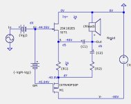
So the pcb is split into a left side and right side. Mosfet on one heatsink, and the SIT on the other. Neat way to keep things cool!
Naturally you want to share the dissipation equally in a project like this. With a (beastly) monaural amplifier, one side of the chassis would be handling the "top half" of the output stage, other side handling the "bottom half". The SIT-1 being another monaural example, with the Static Induction Transistor (and a couple of power resistors) on one heatsink, and a row of six power resistors (100W rated Vishays) on the other to even out the thermal load.
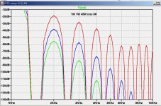
Simulations show that the SIT-5 output stage is amazing. So far I have discovered several major improvements over any of the mu-follower follower MUFF stages:
Also below are spectra for 1W, 7W, and 45W into an 8R load. Very nice.
- Less sensitive to the choice of quiescent Vds of the SIT. Thus it is more tolerant to variations between SITs.
- Distortion falloff pattern remains the same at all power levels. The rate on falloff decreases with power.
- The class-B behavior is excellent at power levels where one of the FETs stops conducting.
Also below are spectra for 1W, 7W, and 45W into an 8R load. Very nice.
Attachments
Welcome in the train!
:--))
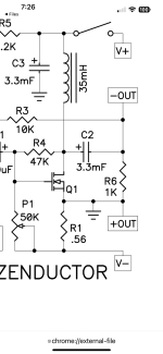
But... I suppose in your draft the contribution of the MOSFET is dominant.
:--))
But... I suppose in your draft the contribution of the MOSFET is dominant.
You are correct that the AC current of PFET is considerably greater than that of the SIT.
But the contribution through C2 is much less than through C1.
The simplified circuit appears to function nicely without R2 and C2. Perhaps the reason for those components is to allow R1 to be big enough for an optocoupler bias circuit but still have strong output from the PFET. No other magic involved.
In the photo you can see electrolytic capacitors rated for 80 volts. I wonder what the power supply voltage is, when delivering 1 watt to a speaker; perhaps it may be 10 or 15 percent less than 80 volts (??)
Generg:
How does one determine the relative contributions from the SIT and the PFET. I do not think that the SIT and PFET currents alone determine the answer without also considering the contributions through C1 and C2.
The bottom line is that I do know really know what the 20% number really means.
How does one determine the relative contributions from the SIT and the PFET. I do not think that the SIT and PFET currents alone determine the answer without also considering the contributions through C1 and C2.
The bottom line is that I do know really know what the 20% number really means.
By looking at the output distortion waveform over the power range—or at least that’s how I imagine Papa did it.
The way the output resistors are connected, one set is used to set the bias and the other can be independently adjusted to ensure that the output character (H2, H3 balance) remains the same over the entire power range. A different way to say this would be that the two resistors in the output are in parallel only for AC.
Another cool thing is that the circuit has BJTs, JFETs, MOSFETs, and SITs, all working together
Yes.
For AC current the PFET is degenerated by the parallel resistance R1||R2.
Thus R1 is used for the bias circuit and R2 adjusts the gm of the PFET.
Very clever.
For AC current the PFET is degenerated by the parallel resistance R1||R2.
Thus R1 is used for the bias circuit and R2 adjusts the gm of the PFET.
Very clever.
By making R2 (the resistor from the PFET source) small, the harmonic spectrum is maintained for 4 Ohm loads.


- Home
- Amplifiers
- Pass Labs
- First Watt SIT5