My plan is transformer > rectifier > Reservoir > Cap Mx .One more question, @Sadface , what is your power source? The usual transformer + bridge rectifier + reservoir caps? And where is it located, mechanically?
Point is, the moment you have ripple on the incoming supply, this ripple is injected into the GND by the regulators' input bypass caps and this can ruin everything, given the very high gain at mains frequencies.
And IMHO there is no benefit from using separate regulators at each opamp for circuit like this. One global set would do.
As for topology, are you sure the rumble filters are at the right location, before the actual input? That isn't a good idea IMHO, for a number of reasons. I'd place them in between the two main stages.
More later....
Mechanically. This will probably go into a salvaged steel chassis of the usual circa 430mm wide. I have an old NAD tuner chassis that looks pretty appropriate.
Mains side on the left. Rectifier + reservoir + cap mx in the middle. Signal as far away as possible to the right.

^ With a LF gain of 1400x (63dB) any tiny design or layout error may easily result in extra hum/buzz that could be louder than record noise. The OP came here to ask if onboard/local regs are OK but that question could easily get irrelevant when other factors are dominating the outcome.
And how to brute-force test if the layout is good at rejecting LF magnetic fields? Tape head demagnetizer ;-)
And how to brute-force test if the layout is good at rejecting LF magnetic fields? Tape head demagnetizer ;-)
Are you not just a little exaggerating? Local regulators won't make matters exactly worse will they? It seems a problem less to worry about. I have built/modified many phono preamps and some were outright noisy but liked best by their owner. Some played back AM radio on the right day and no one judged that to be bad 🙂
Is possible superior technology that much a benefit when we have a nail running through a carved out track in vinyl giving music with a spike here and there?
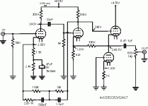
Brute-force testing 😀 Attached is the Hiraga-san phono preamp from 1981.
Is possible superior technology that much a benefit when we have a nail running through a carved out track in vinyl giving music with a spike here and there?
Brute-force testing 😀 Attached is the Hiraga-san phono preamp from 1981.
Attachments
Last edited:
As noted, that depends if there are any ripple return currents through their input bypass caps taking the wrong path back home.Local regulators won't make matters exactly worse will they?
Of course one can always argue "it's just mediocre vinyl playback" so why bother about anything beyond what is deemed "good enough" for that.
However, I have a feeling that @Sadface has some general interest here with redard to good circuit and layout design practices. The foundation (the basic schematic) is good enough for the execution to actually matter.
That is clearly not what I said or meant.
I just wonder if a 4 layer state-of-the-art board made according RF like specifications outperforms a, for instance, 2 tube single layer PCB phono preamp playing back the same record.
I just wonder if a 4 layer state-of-the-art board made according RF like specifications outperforms a, for instance, 2 tube single layer PCB phono preamp playing back the same record.
Last edited:
In terms of measurements, noise/hum/buzz/demodulated RF/etc floor present under the payload signal (idle groove noise) will be much better without any doubt.I just wonder if a 4 layer state-of-the-art board made according RF like specifications outperforms a, for instance, 2 tube single layer PCB phono preamp playing back the same record.
OK. I take "Cap Mx" as cap multiplier, right? At any rate this is a good idea because cap multipliers have high'ish input impedance (the transistors' collectors), reducing ripple current.My plan is transformer > rectifier > Reservoir > Cap Mx .
Here my proposal for a simplified supply arranagement:
Supply ripple return path is factored out and the whole regulator stuff should be localized, like in one corner of the board. Key point is that the single connection to the GND plane is right at the first set of bypass caps, at the C3/C4 junction and not anywhere before that point.
Low ESR bypass caps are used but the regs are kept happy with 1R of isolation which also helps to form a better lowpass filter for all the high frequency stuff that "just jumps over" those lowly regulators. The 1R do degrade load regulation a bit, but there isn't much dynamic load current, if any at all. C7 is for peace-of-mind, making the rails move in union in case some dynamic load current is present. This transforms PSRR of the opamps into CMRR which usually tends to be much better.
Local chip bypasses first combine their GND legs before connection to the GND plane. Output return current thus take the exact same path through the GND plane for both positive and negative currents, even when the output stage should enter class-B operation (where load current appears as half-wave-rectified for each rail).
GND plane is on layer 2 or bottom layer for 2-layers. It should be as continuous as possible, not breaks. Routing a few signal traces for short lengths is OK, though. Free area on top side is also GND plane, connected with stitching vias all over.
With the opamps all lined up in a row a slick supply routing is falling into place naturally and a 2-layer board will suffice, with the supplies on the top layer. Use two wide adjacent strips for each polarity under the chain of opamps, literally forming rails. In the section between the opamps make the strips wider and place the bypasses there, and right below the opamps use all available copper.
But of course 4-layer is more flexible, the strips can be made wider and the overall GND plane conducitivity can be made better (JLC will happily make 4-layer with all layers 1oz copper thickness)
Signal path has been rearranged for a better behavior wrt noise/hum/buzz, IMHO:
1st RIAA/gain stage ==> 1st stage of rumble filter ==> 2nd gain stage ==> 2nd stage of rumble filter, followed by HF RIAA filter and DC blocker
Other arrangements are possible as well as various optimizations but that should not be a topic at this time. However, placing the first gain stage at the input is strongly recommended.
As for that input stage, see following detail:
Last edited:
Interesting suggestions.
I will need to digest that.
Is there much point separating power ground and signal ground when using ground planes?
In a 4 layer design. Might one use 1 layer for signal and 1 layer for power ground?
For example:
top: power rails
inner 1 power gnd
inner 2 signal gnd
bottom signal
I am under the impression that signal grounds are best routed with traces rather than planes to keep currents going where they should be.
There are many ways to skin a cat, as they say.Is there much point separating power ground and signal ground when using ground planes?
In a 4 layer design. Might one use 1 layer for signal and 1 layer for power ground?
For example:
top: power rails
inner 1 power gnd
inner 2 signal gnd
bottom signal
I am under the impression that signal grounds are best routed with traces rather than planes to keep currents going where they should be.
Separate planes for signal and power GND may make sense when there is power (high current) actually involved... which is not the case here. But even with separate planes strong currents in the power plane can still couple magnetically to the reference GND plane and pollute it.
IME, for the kind of circuits at hand (line signal levels, audio frequencies, low currents) the simple "copper block" approach is fully sufficient if not overkill already.
Pour everything with GND copper, stitch it together across layers with tons of vias. One layer should have as continuous a GND plane as possible.
Carve out the signal tracks. Make pos and neg supply tracks wide (low inductance) and keep them close together and over closed GND plane (low inductance, again).
Put all connectors and the power input to the PCB on one edge. Not current other than signal current (and signal return current reflected in the rails) shall flow across the PCB.
And for high gain circuits, check and minimize magnetic loop pickup area. Sometimes a simplified intermediate drawing may help, bridging the gap from schematic to actual layout.
From a high-level perspective there's no difference between those two solutions. At the lower level you could argue that if you kept the left channel inside one opamp and the right channel inside another there'd be better channel separation. But as I pointed out earlier, channel separation is not your chief concern in a phono stage.I mean using 2 halves of an OPamp for one channel vs 1/2 for each channel.
A dual opamp is literally two identical opamps on the same die. Sometimes the bias circuitry and other housekeeping stuff is shared between the two amps, but not always.
You might be able to save yourself a bit of time by looking at the rats nest more closely during the component placement stage. The curved nets feature in KiCAD can be helpful here.I also love designing pcbs. A new design normally keeps me busy for weeks playing Tetris and speccing the various parts.
Next up I will move the OPamps around and see if I can make a better layout with each channel having its own 2 opamps instead of 4 shared ones as above.
I prefer to move the components around before I connect any tracks. Get the placement right, then route. That doesn't mean I don't sometimes change the component placement during routing, but that tends to only happen in small areas.
Just a thought. I'm not suggesting there's a right way and a wrong way.
Tom
Where do the regulators go then?My plan is transformer > rectifier > Reservoir > Cap Mx .
I'm assuming that by "Cap Mx" you mean cap multiplier. Note that those work well until the incoming power glitches. Then the capacitor is discharged by the output current. The cap multiplier has no ripple rejection while the capacitor charges, so once the incoming power recovers you'll get hum fed through the multiplier.
If you want to use a capacitor multiplier you need to design it such that it drops sufficient voltage to handle brownouts on the incoming AC voltage. That makes for a pretty lossy non-regulator.
If ripple rejection is your top concern, just use one of the more modern regulators such as the TPS7A49 and TPS7A30.
And as pointed out by others already, there's no need for separate regulators for each opamp. In fact, that could end up hurting you as you will then have to route the unregulated voltage all across the board, so it's free to couple into any inductive loop you have available.
For the physical layout, i.e., placement of board(s) within the chassis: Keep in mind that the charging currents that run in the transformer, rectifier, and reservoir capacitors are pulses of pretty high magnitude. A pulse has lots of high frequency content so it will happily couple into just about anything. Keep the amount of reservoir capacitance reasonable and keep the transformer, rectifier, and reservoir capacitors away from any sensitive audio circuitry.
Do read that "G Word" article that Jan linked to earlier. The PCB layout on the last page shows you how it's done. Bruno does good work.
Tom
You don't need 4 layer board. 2 layer is sufficient.
If you can don't mix audio ground with power ground.
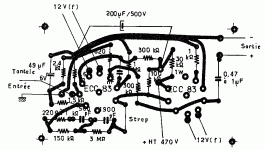
Look at this:
audio ground connects with power ground only in power socket (3 pin, on the right side in the middle).
Right side = regulators LM317/337 with a few caps.
Decoupling caps close to opamp pins between rails.
Top layer = ground
Bottom = signal traces
If you can don't mix audio ground with power ground.
Look at this:
audio ground connects with power ground only in power socket (3 pin, on the right side in the middle).
Right side = regulators LM317/337 with a few caps.
Decoupling caps close to opamp pins between rails.
Top layer = ground
Bottom = signal traces
Attachments
That's one way to do it. You can do the same with a ground plane, but you'll have to visualize the current densities in the plane or use an EM field solver to show you. I use ground planes a lot.I am under the impression that signal grounds are best routed with traces rather than planes to keep currents going where they should be.
True. But one layer is sufficient too. Just add some wire jumpers. That's done a lot in cheap overseas manufacturing.You don't need 4 layer board. 2 layer is sufficient.
Four layer boards are dirt cheap these days, so if using four layers makes life easier I'd recommend four layers.
Tom
Ya'll folks are beginning to convince me that separate regulators per opamp is probably not the best way forward.
I am not married to the idea, it was simply an interesting thing to play with.
I've been playing with the layout a bit these last 2 nights. Placing the opamps in a line with power rails straight down the middle does allow quite a nice clean looking layout. I'm also playing with TH resistors again which while large do often simplify the layout due to acting as jumpers over traces.
We'll see how I go with TH vs SMD resistors. I might flip back the other way again.
In regards to power supplies. The TPS7A reg's do look nice but are not cheap from ali express in slightly dubious premade form and soldering packages that tiny is out of my capabilities with my current tools etc.
A VRDN is certainly not however and gives stellar performance from stuff I have on hand anyway. So perhaps this is the way to go.
I've been wanting to play with a Cap Mx before a reg for a while and this one is still on the agenda so perhaps a modified VRDN with Cap Mx instead of the bulk capacitance is the way to go.
It probably can be just fine if taken into the context of having preregulators distributing already regulated voltages. This was once a method by a few brands in the phono era when part costs were less relevant. Likely a more effective approach than using cap multipliers in such a low current device. When you decide to use single opamps you can be sure they don’t have influence on eachother.
Maybe it is a good idea to just design it the way you think it is good and test it. The impression is that you otherwise get tangled in new ideas or insights and no preamp will be realised.
Maybe it is a good idea to just design it the way you think it is good and test it. The impression is that you otherwise get tangled in new ideas or insights and no preamp will be realised.
Last edited:
I think I have done this crudely right:Signal path has been rearranged for a better behavior wrt noise/hum/buzz, IMHO:
1st RIAA/gain stage ==> 1st stage of rumble filter ==> 2nd gain stage ==> 2nd stage of rumble filter, followed by HF RIAA filter and DC blocker
Other arrangements are possible as well as various optimizations but that should not be a topic at this time. However, placing the first gain stage at the input is strongly recommended.
As for that input stage, see following detail:
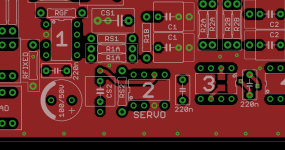
View attachment 1364749
No parts designations have been changed

Input RF filter added
Why on Earth would you buy them at AliExpress? TI will happily sell them to you directly. They usually ship from Singapore, so it shouldn't take long for them to deliver.The TPS7A reg's do look nice but are not cheap from ali express
There's always Mouser, Digikey, Farnell/Newark, etc. as well. I see no compelling reason to shop at grey/black market vendors for this.
Tom
Probably. I trust that you've run a circuit sim to see if you get the frequency response you want.I think I have done this crudely right:
One note: Sallen-Key filters don't make the best use of the available loop gain. I suggest taking a look at multiple-feedback filters: https://www.ti.com/lit/an/sloa049d/sloa049d.pdf
Tom
- Home
- Amplifiers
- Power Supplies
- Regulators right beside OPamps pins