I have seen many versions of P3A on the net incl. the original Rod Elliot's PCB. I'm just wondering that whether Rod's layout has a "Star ground" or not. All I can see is a straight copper track with various components soldered along the bottom track with the main power gnd located right in the middle PCB
Disclaimer - I'm not an expert in PCB designing
Disclaimer - I'm not an expert in PCB designing
Hi, do you have thé pcb layout?Hello Nikos, have you sent this lay-out to a pcb house? A few thoughts, input source should be away from power sources, yours is very close to rail fuse. another preference of mine is 'rail fuses is placed as part of the PSU board'. One acceptable consideration is 'placing the rail fuses in between a stereo board, just like Rod Elliotts pcb design.
This is my personal preference of a CFP output amp board. Outputs, drivers and zobel network is placed near each other, the more compact the better.
I remember you made a pcb for the P3A and you were satisfied by the
result.
Regards
^follow this you tube video, the PCB lay-out used by the presenter was a design I created for P3A. A link to the gerber file (google drive) iss provided in the description. Check first using a gerber viewer and you can see my old sign 'Abetir' (but I guess a slight mod is done more likely to accomodate some replacement devices).

Layout is not a real big factor for a design like the P3A. By no means is it a PPM amp !
It's going to test at .01-02% however it is lay'ed out. As long as NFB takeoff is correct and
there are no gross electrical mistakes. Even a less than ideal star ground would not matter with this
design.
Elliots designs are inspiring , but most of the present DIYA designs are light years ahead.
OS
It's going to test at .01-02% however it is lay'ed out. As long as NFB takeoff is correct and
there are no gross electrical mistakes. Even a less than ideal star ground would not matter with this
design.
Elliots designs are inspiring , but most of the present DIYA designs are light years ahead.
OS
I checked with online gerber viewer, its showing blank, no layers or am I missing something. If possible, can you post your gerber files over here please.Check first using a gerber viewer
Secondly, can this same P3A PCB also work with A1106 C2581output transistors ?
Attachments
Sorry, I couldn't understand the meaning of PPM, I'm total noobs to solid state design acronymsBy no means is it a PPM amp !
It's going to test at .01-02%
parts per million.
0,0001 % = 1 PPM
This is a very old project that I made, so sorry I could no longer find my files. I think I have replaced my PC four times already. I must've erased the files in the process. Try to PM member Nikos, I think he still have my unmodded files.can you post your gerber files over here please.
Secondly, can this same P3A PCB also work with A1106 C2581output transistors ?
As I am not the designer I cannot answer for the use of A1106/C2581 transistors. My recommendation is to stick with the parts values per the original schematic. You could possibly replace the original devices provided that their specs is very close to that of the original devices. I may have to CAUTION you, this amplifier is CFP output If you are an unexperienced builder you could possibly end up doing harm to the amplifier in the process.
Hi availlyrics, the PCB in pdf from de Ocampo is here:
https://www.diyaudio.com/community/threads/rod-elliot-p3a-layout-critics.201446/page-18#post-5122537
https://www.diyaudio.com/community/threads/rod-elliot-p3a-layout-critics.201446/page-18#post-5122537
you are right in your observations, I'm a noob to SS amplifier build , as my previous builds were usually chipamps. I have also 21193/94 , which I'm going to try first. I was just wondering if A1106 C2851 can work on lower supply voltages as a backup, incase I manage to blow up the recommend transistors.I may have to CAUTION you, this amplifier is CFP output If you are an unexperienced builder you could possibly end up doing harm to the amplifier in the process.
Don't worry, I have variac, scope, speaker protection circuit, etc. Just needed to clear my doubts from more experienced FMs like you
^..when in doubt just hit the 'search button' a lot was already discussed with P3A posted from various threads/topics. My first P3A built using my lay-out worked like a charm. 😉
CFP output stages are "picky". Device Hfe (gain) , Cob (base capacitance) are a big factor in the resultant stability.My recommendation is to stick with the parts values per the original schematic.
The original sourcing resulted in working amps , go with it.
OS
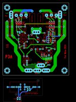
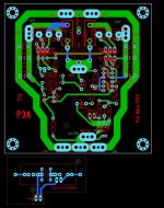
Can you please post pdf of your PCB layout , for toner transfer methodLast version without fuses.
- Home
- Amplifiers
- Solid State
- P3A PCB Layout