how it was translated going from 2 to 4 at listening checking ? Did you ABX it ?
T.I. says in their litterature than stargrounding when a standalone DAC chip can be good. Of course, in this kown scenario, the star is pin 5, only (but for the digital signals but here pin 14 has its autobahn to pin 5). It was John Brown analys who made sorta of "paths towards pin 5 (but anyway currents mix more or less at one moment. One path from the 14 DEM, One for the -15V and one for the DGND. Of course you had to understood what happened with the PS line and close lythic caps decoupling (many didn't).
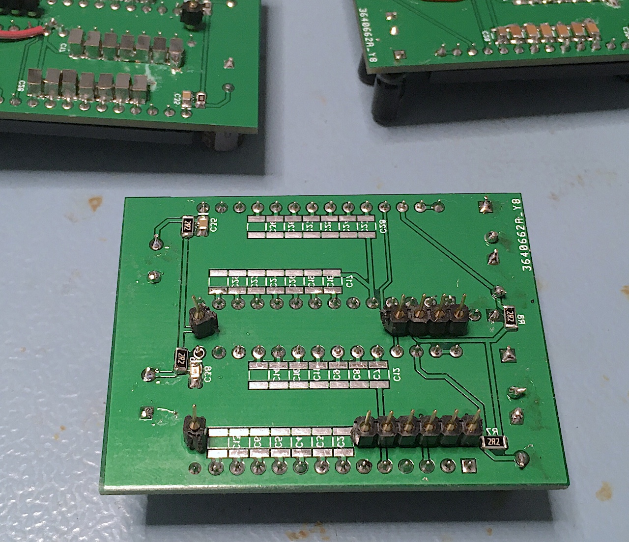
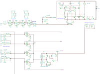
I try to finish the DEM sync before sending you the layers details. SMD decouplings in the above pictures are 1205 size.
T.I. says in their litterature than stargrounding when a standalone DAC chip can be good. Of course, in this kown scenario, the star is pin 5, only (but for the digital signals but here pin 14 has its autobahn to pin 5). It was John Brown analys who made sorta of "paths towards pin 5 (but anyway currents mix more or less at one moment. One path from the 14 DEM, One for the -15V and one for the DGND. Of course you had to understood what happened with the PS line and close lythic caps decoupling (many didn't).
I try to finish the DEM sync before sending you the layers details. SMD decouplings in the above pictures are 1205 size.
Last edited:
how it was translated going from 2 to 4 at listening checking ?
Blind listening between multiple players, same CD loaded and reacting to commands from the same remote.
Questionaires for preference and grading of percieved fidelity impairments.
Did you ABX it ?
Of course not. ABX is cargo cult science, no worse, it is an intentional confidence trick based fraud worthy of any carnival sideshow ripping of the consumers or of the "Great Randi"
T.I. says in their litterature than stargrounding when a standalone DAC chip can be good.
Depends on the DAC chip. It is useless talking in generic terms unless we talk about generic items.
Of course, in this kown scenario, the star is pin 5
It is the best option if we use the classic design.
But it works well with an AGND plane for all PSU decoupling and DEM Cap decouling with a wide trace from the plane centre to pin 5 and DGND to Pin 5.
It was John Brown analys who made sorta of "paths towards pin 5 (but anyway currents mix more or less at one moment. One path from the 14 DEM,
One for the -15V and one for the DGND. Of course you had to understood what happened with the PS line and close lythic caps decoupling (many didn't).
I always used copper planes in hardwiring, CD-77 first generation used star ground, MK II never made it into MP, but returned to copper planes..
I try to finish the DEM sync before sending you the layers details. SMD decouplings in the above pictures are 1205 size.
The DEM sync part at the TDA1541 is simple.
2 X 1nF on 16/17 (can be 0603) and a 330R resistor.
This gives a functional oscillator with 500pF and a slightly increased resistance from 1800 (+/-25%) to 2175 (+17/-18%), so 1 / 5.9 (R *C) ~ 156 kHz.
The sync signal is applied differential across the 330R resistor, via series resistors depending on source signal swing. These resistors should be at the source and use a slew rate limit similar to the digital signals.
So ideally we have 6 X SMA connector (I hate FL).
Thor
Clever. Hopefully it will be stable with only 10n at T3 emitter, microcap was showing that 10R + 10n works well. BTW it's important to check transients with a small time step on the spice settings, such as 10ps and fast risetime square wave (1ns).
(Am I being overly cautious? What is the worst case TDA1541A slew rate?)
This capacitor is of course subject to in circuit optimisation.
But I went back to an earlier concept, after I found the "magic trick".
I realised that I have enough voltage in hand to cascode the current conveyor in the first stage. In the second stage the trick was to separate out the first emitter follower and drive the Sallen Key filter from that point and to then add the phase-splitter for a balanced output.
Again, the 10n capacitor and operating points etc. may need optimising in the real circuit with the real transistors. In the Sim I used BC327/337 from the TINA Library.
Thor
T.I. says in their litterature than stargrounding when a standalone DAC chip can be good. Of course, in this kown scenario, the star is pin 5, only (but for the digital signals but here pin 14 has its autobahn to pin 5). It was John Brown analys who made sorta of "paths towards pin 5 (but anyway currents mix more or less at one moment. One path from the 14 DEM, One for the -15V and one for the DGND. Of course you had to understood what happened with the PS line and close lythic caps decoupling (many didn't).
From here:
Sound decoupling caps TDA1541a
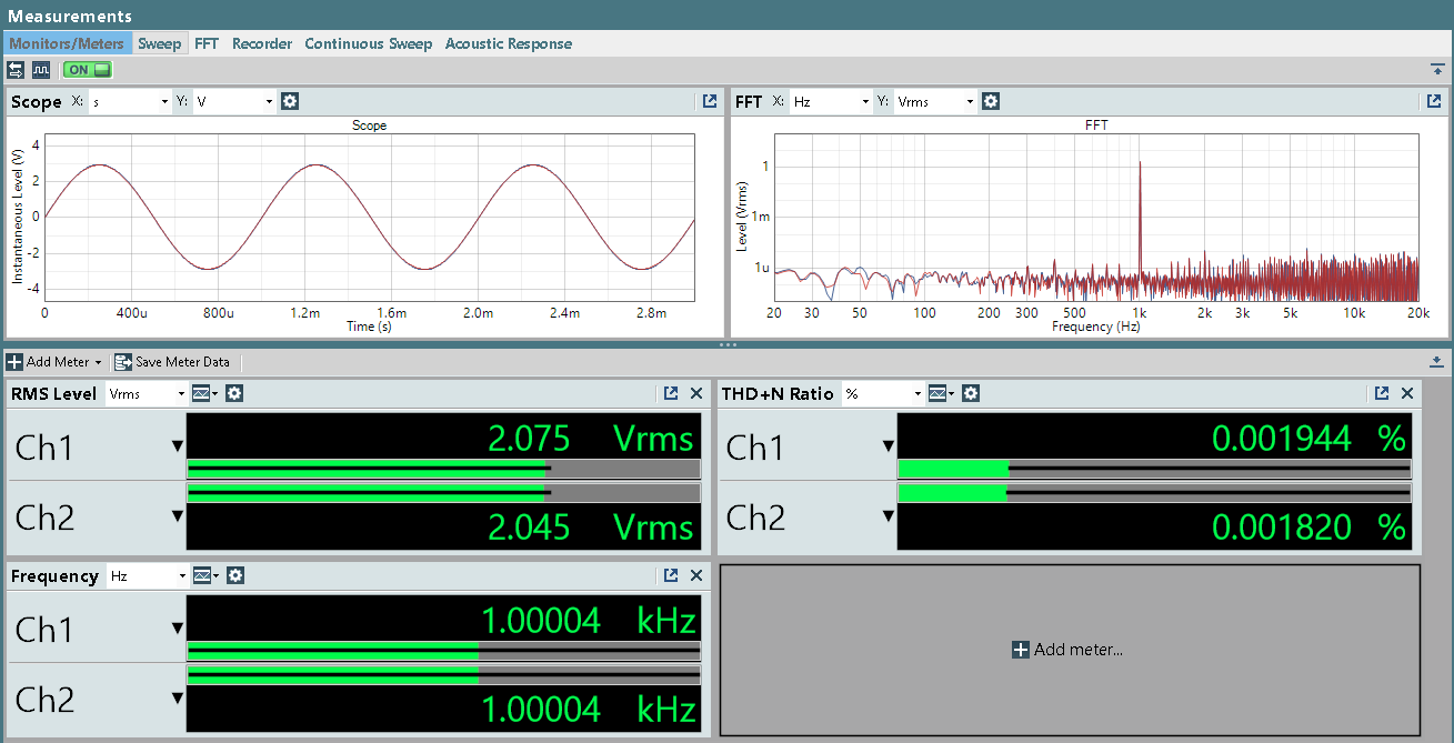
THD-N with SMD star-ground

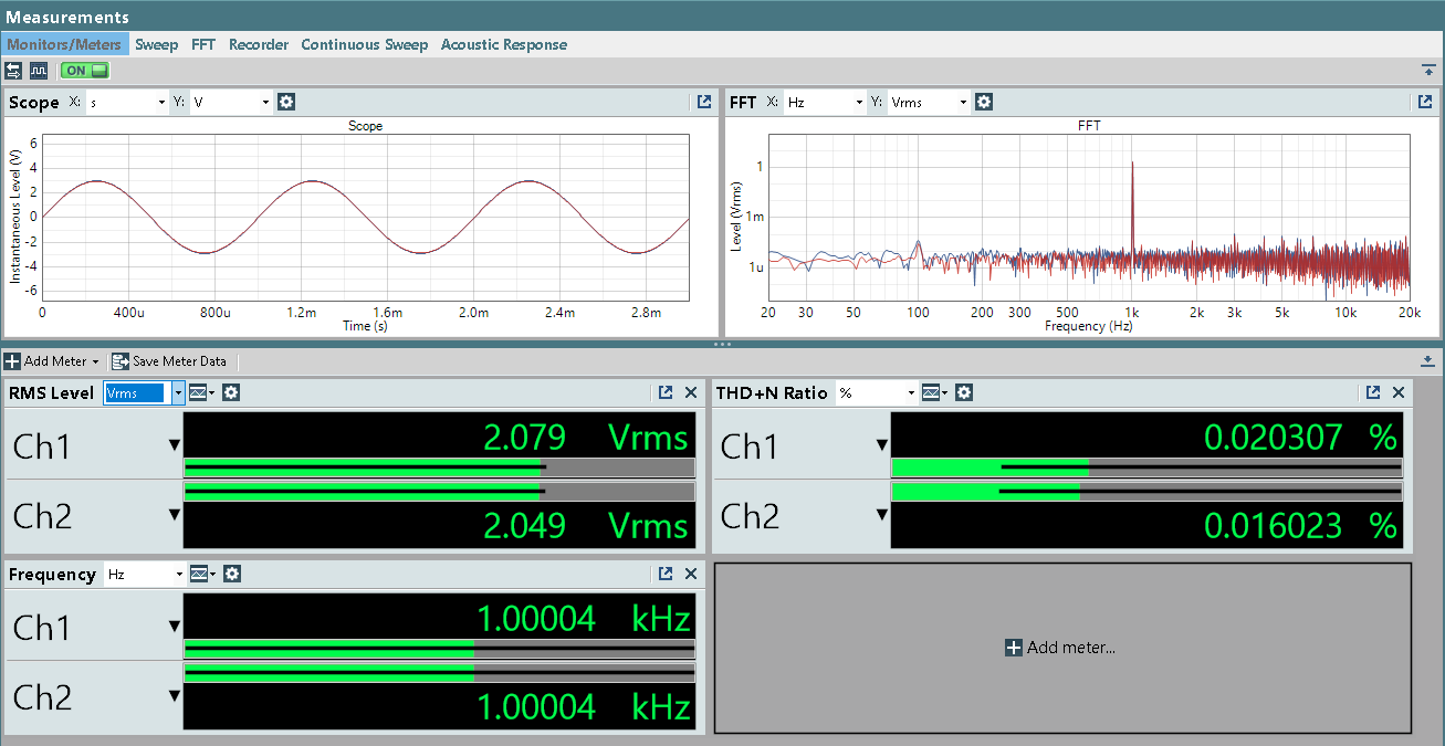
Here THD-N with SMD connect to ground plane, little better

Measured with 1 kHz unditherd 0 dBfs , Ceramic capacitors
Also:
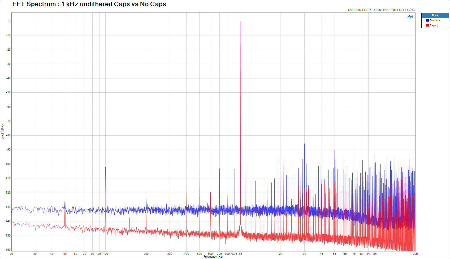
I made a third board with out caps
1 kHz Capacitors no dithered
1 kHz no Capacitors no dither
1 kHz 0 dBfs no capacitors VS Capacitors no dither 20- 20 kHz
1 kHz 0 dBfs no capacitors VS Capacitors no dither 20- 96 kHz
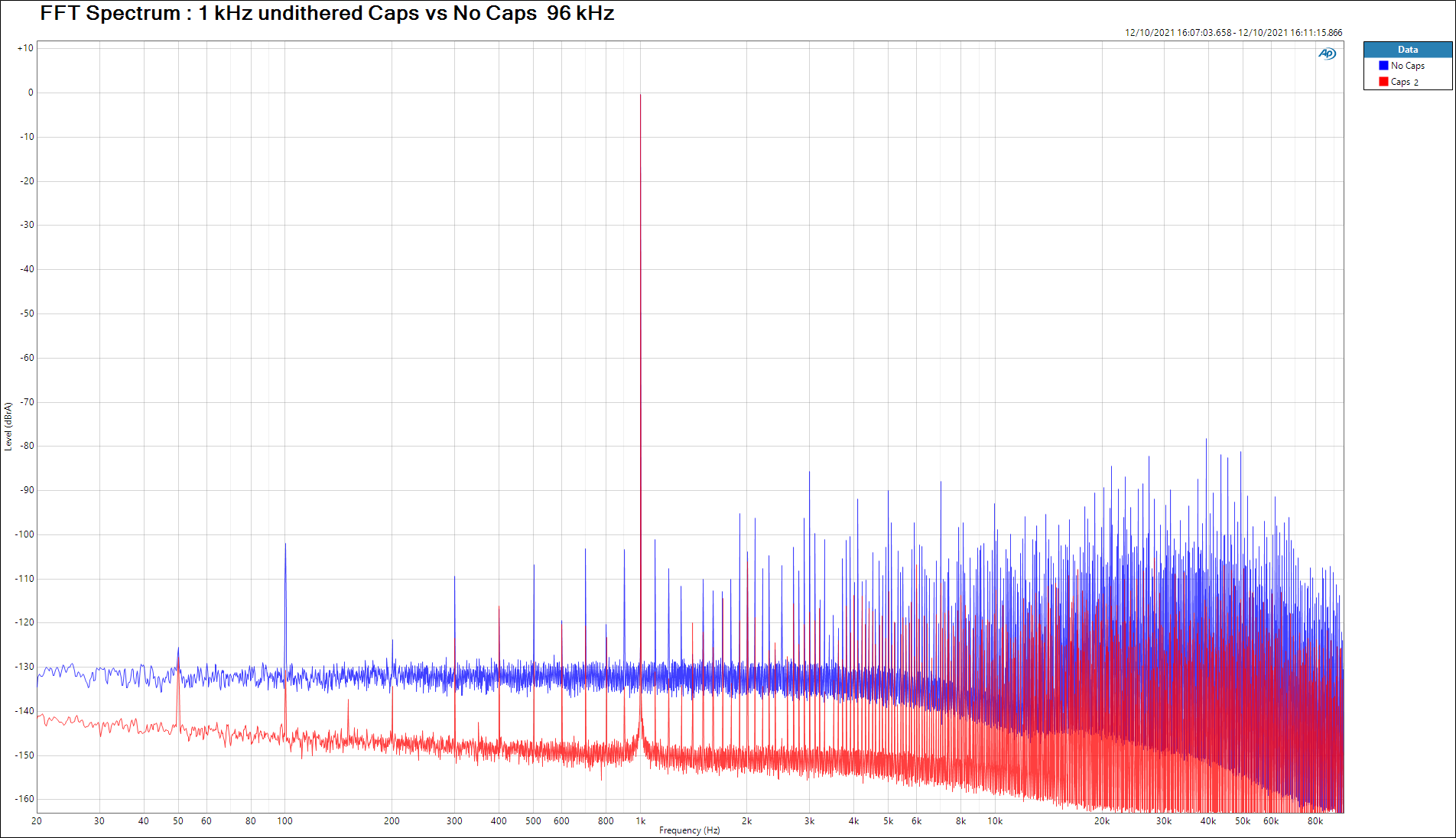
Quite interesting.
More interesting stuff all over the site... I like this bit:
Building Staggerd DAC upgrade basesed on CDX1144/1244 and TDA1541A DAC
8 x Over Sampling TDA1541a – CXD 1244 ?
Here is a job for a CPLD/FPGA to combine with 16 MSB & 16 LSB split and simultaneous mode output (needs 4 TDA1541) for a 32Bit/768kHz TDA1541...
Thor

I talked about the 3 main power rails not the 14 DEM caps. Btw AMR and Audial used both Panasonic PPS here , more expensive than C0G less precise and less stable on the capacitance values after soldering. (2 to 5 % at best).
Hi
Wha is the definite decoupling values, and schematic?
Because we have more than 3 different?
.
first for dem pins:
1.

2.
07 / 24 - DEM LSB - 0.047uF/1206 to VEE1 (GCM31M5C1H473JA6L)
08 / 23 - DEM BIT6 - 0.047uF/1206 to VEE1 (GCM31M5C1H473JA6L)
09 / 22 - DEM BIT5 - 0.047uF/1206 to VEE1 (GCM31M5C1H473JA6L)
10 / 21 - DEM BIT4 - 0.1uF/1206 to VEE1 (GCM31C5C1H104JA16K)
11 / 20 - DEM BIT3 - 0.22uF/1206 to VEE1 (GRM31C5C1H224JE2L)
12 / 19 - DEM BIT2 - 0.47uF/1206 to VEE1 (GRM31C5C1E474JE1L)
13 / 18 - DEM MSB - 2 X 0.47uF/1206 to VEE1 (GRM31C5C1E474JE1L)
---------
power pins decoupling:
1.

2.

3.

4. (just power pins and those related to them)
.
05 - AGND - 0.47uF/1206 to VEE1 (GRM31C5C1E474JE1L)
06 - AOR - 0.01uF/1206 to VEE1 (GRM3195C1E103JA1D)
14 - DGND - 0.47uF/1206 to VCC (GRM31C5C1E474JE1L)
15 - VEE1 (-15V) - 0.47uF/1206 to AGND (GRM31C5C1E474JE1L)
25 - AOL - 0.01uF/1206 to VEE1 (GRM3195C1E103JA1D)
26 - VEE2 (-5V) - 0.47uF/1206 to VEE1 (GRM31C5C1E474JE1L)
27 - FMT - link to VEE2
28 - VCC (+5V) - 4 X 0.47uF/1206 to VEE1 (GRM31C5C1E474JE1L) - 0.47uF/1206 to DGND (GRM31C5C1E474JE1L)
Thaks 🙂
Wha is the definite decoupling values, and schematic?
Because we have more than 3 different?
.
first for dem pins:
1.
2.
07 / 24 - DEM LSB - 0.047uF/1206 to VEE1 (GCM31M5C1H473JA6L)
08 / 23 - DEM BIT6 - 0.047uF/1206 to VEE1 (GCM31M5C1H473JA6L)
09 / 22 - DEM BIT5 - 0.047uF/1206 to VEE1 (GCM31M5C1H473JA6L)
10 / 21 - DEM BIT4 - 0.1uF/1206 to VEE1 (GCM31C5C1H104JA16K)
11 / 20 - DEM BIT3 - 0.22uF/1206 to VEE1 (GRM31C5C1H224JE2L)
12 / 19 - DEM BIT2 - 0.47uF/1206 to VEE1 (GRM31C5C1E474JE1L)
13 / 18 - DEM MSB - 2 X 0.47uF/1206 to VEE1 (GRM31C5C1E474JE1L)
---------
power pins decoupling:
1.
2.
3.
4. (just power pins and those related to them)
.
05 - AGND - 0.47uF/1206 to VEE1 (GRM31C5C1E474JE1L)
06 - AOR - 0.01uF/1206 to VEE1 (GRM3195C1E103JA1D)
14 - DGND - 0.47uF/1206 to VCC (GRM31C5C1E474JE1L)
15 - VEE1 (-15V) - 0.47uF/1206 to AGND (GRM31C5C1E474JE1L)
25 - AOL - 0.01uF/1206 to VEE1 (GRM3195C1E103JA1D)
26 - VEE2 (-5V) - 0.47uF/1206 to VEE1 (GRM31C5C1E474JE1L)
27 - FMT - link to VEE2
28 - VCC (+5V) - 4 X 0.47uF/1206 to VEE1 (GRM31C5C1E474JE1L) - 0.47uF/1206 to DGND (GRM31C5C1E474JE1L)
Thaks 🙂
yep, I made it based on this post too. https://www.diyaudio.com/community/...ate-nos-dac-using-tda1541a.79452/post-7763090
when you have more than one smd C0G it is easy to stack on the 1205 pads size; I personnaly always solder the caps on their side; this way two sides to sides is feasible according the thickness of the body (voltage rating)
Edit, your FDEM sync is different from Thorsten's ( 16xWck ; not took from MCK).
Which shematic applies (register ref), I am onthe two registers shematic of Thorsten.
That's why I make first a core pcb with just the local final decoupling (and eventually FDEM took from Bck / by shift registers ?)
Attachments
Last edited:
Maybe it will be usefull, I think that these NPO smd-a are good too?
https://datasheets.kyocera-avx.com/C0GNP0-KGM.pdf
https://datasheets.kyocera-avx.com/C0GNP0-KGM.pdf
Why not sync to the IIS BCK which is present before the IIS2SIM converter?
You can use MCK of course, but then your DEM Clock becomes 4 X the highest sample rate. This creates an overhead of (very) high frequency (VHF) disturbances in the system not needed for lower sample rates.
There is evidence that 64 X DEM clocks work ok, I might suggest in this case trying 64 X as DEM clock and minimal (1nF?) or no DEM filter capacitors.
Hello,
Very interesting and thank you, I would like to ask please:
Synch DEM to I2S BCK (64Fs) and /16 so fDEM = 4xWS for all input sample frequencies vs synch to simdata BCK (32Fs) and /8 for fDEM = 4xWS (for all inputs).
Fundamentally the same, or a reason to prefer synch to I2S BCK before the I2StoSIM conversion?.
John
@ThorstenL
About the external dem for 16 / 17 pins, from the answers, is only sure that it should be present all of the time.
Regardless of the input digital data formats.
.
In I2S mode:
MCK and BCK are present all of the time.
MCK has fixed value (2 values for 44.1/48KHz base SR), but it is fixed. doe not changed with SR change.
BCK is changing according to SR (and it is derived from MCK.)
It is present at the input format.
.
MCK has to be present on any translator I2S-to-TS board.
In TS mode BCK is in stoped operation mode, it is NOT present "all" the time.
So the use of adaptive dem 16 / 17 pins, Fo, for 4 x SYNC
ONLY with I2S BCK preset at the input of I2S-TS boards...
That will introduce the 5th input line in the on the TDA PCB:
LE, DATA, BCK_TS, MCK for recklocking and BCK_i2S
And some physical intervention on I2S-TS boards in term to managing the cable sygnal from input I2S BCK line...
.
.
.......
.
I am asking all this because, I would like to try this external dem, with Sine signal.
To compare to square signal?
And if the Fo of dem is changing a lot, the Square to sine passive RC circuit has to change too.
So that complicate that option a lot. It is not impossible but it deserves information about SR to manage divide and to switch the
.
Anyway someone have to made some real world simple experiments, measure/ listen and report about...
About the external dem for 16 / 17 pins, from the answers, is only sure that it should be present all of the time.
Regardless of the input digital data formats.
.
In I2S mode:
MCK and BCK are present all of the time.
MCK has fixed value (2 values for 44.1/48KHz base SR), but it is fixed. doe not changed with SR change.
BCK is changing according to SR (and it is derived from MCK.)
It is present at the input format.
.
MCK has to be present on any translator I2S-to-TS board.
In TS mode BCK is in stoped operation mode, it is NOT present "all" the time.
So the use of adaptive dem 16 / 17 pins, Fo, for 4 x SYNC
ONLY with I2S BCK preset at the input of I2S-TS boards...
That will introduce the 5th input line in the on the TDA PCB:
LE, DATA, BCK_TS, MCK for recklocking and BCK_i2S
And some physical intervention on I2S-TS boards in term to managing the cable sygnal from input I2S BCK line...
.
That is why I was asked about... As only option left with TS format. 🙁 IF we want that dem to be in sync with BCK and continuous...Why not sync to the IIS BCK which is present before the IIS2SIM converter?
.
.......
.
I am asking all this because, I would like to try this external dem, with Sine signal.
To compare to square signal?
And if the Fo of dem is changing a lot, the Square to sine passive RC circuit has to change too.
So that complicate that option a lot. It is not impossible but it deserves information about SR to manage divide and to switch the
.
Anyway someone have to made some real world simple experiments, measure/ listen and report about...
For DEM @ 16 / 17 pins there is the formula with function of frequency.
.
Probably the formula for F as function of Cs at the DEM BITs pins exist too?
Someone have information about that?
.
Probably the formula for F as function of Cs at the DEM BITs pins exist too?
Someone have information about that?
More interesting stuff all over the site... I like this bit:
Building Staggerd DAC upgrade basesed on CDX1144/1244 and TDA1541A DAC
8 x Over Sampling TDA1541a – CXD 1244 ?
Here is a job for a CPLD/FPGA to combine with 16 MSB & 16 LSB split and simultaneous mode output (needs 4 TDA1541) for a 32Bit/768kHz TDA1541...
Thor
Here is more ,
CXD 1144A vs CXD 1244
https://www.bramjacobse.nl/wordpress/?p=9134
I talked about the 3 main power rails not the 14 DEM caps. Btw AMR and Audial used both Panasonic PPS here , more expensive than C0G less precise and less stable on the capacitance values after soldering. (2 to 5 % at best).
At the time we did our design, C0G did not come in large enough values. Nowadays I recommend and use C0G.
MK II was to use C0G.
Thor
Wha is the definite decoupling values, and schematic?
For a newly spun PCB, the C0G capacitors with explicit part numbers.
All else is my "development diary" for my own build, for which I will use the parts in stock or already purchased.
Thor
Fundamentally the same, or a reason to prefer synch to I2S BCK before the I2StoSIM conversion?.
Many (or all) SIM output devices implement "stopped clock" mode with BCK = 32 X WCK, which is pointless bordering on moronic, on the principle that a half duration of louder and higher pitched noise is better than a lower pitch and lower level continuous noise.
Hint, fix the noise problem instead?
Thor
I am asking all this because, I would like to try this external dem, with Sine signal.
The oscillator is not sinewave. Just look at the Schematic of it and the sawtooth waveform of the actual OSC pin's in free running operation.
What do you hope to gain using a sinewave?
Don't tell me you also want to use a Tube LC oscillator to drive the DEM pins with a sinewave.
Use a clipped (level limited) and slew rate limited (< 10nS/V) squarewave. That will work much better that a sine.
Thor
Probably the formula for F as function of Cs at the DEM BITs pins exist too?
Someone have information about that?
Kind of. We can determine the minimum.
There is as such no maximum on capacitance. We see 100nF (standard CDP) to 680uF (MVAL) on the MSB.
We need to consider the worst case peak-peak ripple current, which is Iref / 4 * 10%.
We need the switching frequency and on each pin and the worst case ripple current.
In every group of 3 pins we have:
2 * I & Fdem / 2 on the MSB,
I & Fdem on the middle pin.
and I / 2 & Fdem / 2
Pin 3 is also the MSB in the next group of 3.
Or we have:
1 IrF - Group 0
1/4 IrF - Group 0
1/4 IrF - Group 0 / Group 1 MSB
1/16 IrF - Group 1
1/16 IrF - Group 1 / Group 2 MSB
1/64 IrF - Group 2
1/64 IrF - Group 2
So if we have a value of X for C bit 0 (MSB) and then minimum values of:
C0 = C0 / 1
C1 = C0 / 4
C2 = C0 / 4
C3 = C0 / 16
C4 = C0 / 16
C5 = C0 / 64
C6 = C0 / 64
New realisation, there is a geometric progression here, but it is C0 (MSB Cdem) that is critical and the geometric progression is not "each next C 1/2 the preceding value" even though this works at keeping the values above minimum.
The next challenge is to determine C0 min.
We need the variation from the ripple current (2.5% of 2mA worst case) cause less voltage variation across C0 (MSB Cdem) than 1/2 MSB respective to the nominal voltage across C0, which is ~7.5V.
So when does a PP current of 50uA produce 1/(2^17) or 0.000007629 of 7.5V or less?
When the impedance of the capacitor C0 at Fdem/2 is such that 50uA ripple produce 57uV or less ripple.
This suggest that the impedance of C0 should be < 1 Ohmm @ Fdem.
Let's assume Fdem = 176.4kHz.
Zc = 1 / (2 * PI() * F * C)
Zc = 1
thus
1 = 1 / (2 * PI() * F * C)
thus
2 * PI() * 176400 * C = 1
thus
C = 1 / 2 * PI()* 176400 (or Fdem)
C = 1 / 1108354
C = 0.9uF
A piece of evidence in support of the 1uF value:
This circuit is from one of the fional TDA1541 designs ever done, a digital satellite radio tuner designed by Grundig for Philips, we see 1uF on MSB. We do not see 220nF on the next two though, but we often see all 220nF in upper end TDA1541 Designs.
If we use high frequency Fdem synchronised with WCK, we probably can relax the minimum value, as we always reliably average a whole cycle so the net ripple is ALWAYS zero and the remaining ripple is averaged out by the analogue stage.
If we do not relax requirements, we find (using standard values), for a minimum sample rate of 44.1kHz and Fdem = 4 X WCK
C0 = 1uF (or 0.94uF from 0.47uF C0G in parallel)
C1 = C2 = 270 or 220nF
C3 = C4 = 68nF
C5 = C6 = 15nF
In practice, based on the above I'd use for 176.4kHz Fdem (or minimum Fdem):
C0 = 2 X 470nF C0G // or 1uF Film // 100nF C0G
C1, C2 = 220nF C0G or 2 X 100nF //
C3,4,5,6 = 100nF C0G
Incidentally, for 60Hz it becomes 2650uF and for 120Hz we need 1325uF.
So for 120Hz:
C0 = 2 X 680uF KL 35V
C1,2 = 330uF/470uF KL 50V
C3,4 = 100uF KL 100V
C5,6 = 22uF KL 100V
Now all the above is based on the absolute worst case current ripple, which in real IC's likely affects at best 1 in 100 IC.
So lower values in practice are unlikely to cause big trouble, but I'd not go below half the theoretical minimum value, or a quarter if we use Fdem = 4 X WCK or integer multiples.
At the same time, as said, if it does not cause lower quality capacitors to be used, using larger values is not a problem.
Lastly, remember each DEM Filter capacitor pin has narrow glitches at Fdem that are about 50 - 100MHz equivalent frequency, so RF behaviour of these capacitors is important.
Thor
Hello - beer for you, on me (life is good enough_watch space)Many (or all) SIM output devices implement "stopped clock" mode with BCK = 32 X WCK, which is pointless bordering on moronic, on the principle that a half duration of louder and higher pitched noise is better than a lower pitch and lower level continuous noise.
I understand this, yet. If you want 384kHz - simdata mode input is necessary - all previous and not to shoot the somewhat rising SNR thread in the bollocks... so you have simdata input, or not?
You say you want 384k - no?.
_if so.. my question stands _ take BCK 32Fs /8 .., for fDEM. vs I2S BCK 64Fs /16 = same, same. Or same, Lion.
Cheers to you and thanks for what you do. \\
Last edited:
I never understood why the MSB decoupling capacitor (and some bits below) should be bigger capacity than the rest. I have done extensive experiments with the decoupling pins ripple and sensitivity to "artifical" leakage current (using an adjustable current source) and I can say that all decoupling pins have the same sensitivity, same internal impedance, same ripple without capacitor, they are same in every aspect.Hi
Wha is the definite decoupling values, and schematic?
Because we have more than 3 different?
.
first for dem pins:
1. View attachment 1350436
2.
07 / 24 - DEM LSB - 0.047uF/1206 to VEE1 (GCM31M5C1H473JA6L)
08 / 23 - DEM BIT6 - 0.047uF/1206 to VEE1 (GCM31M5C1H473JA6L)
09 / 22 - DEM BIT5 - 0.047uF/1206 to VEE1 (GCM31M5C1H473JA6L)
10 / 21 - DEM BIT4 - 0.1uF/1206 to VEE1 (GCM31C5C1H104JA16K)
11 / 20 - DEM BIT3 - 0.22uF/1206 to VEE1 (GRM31C5C1H224JE2L)
12 / 19 - DEM BIT2 - 0.47uF/1206 to VEE1 (GRM31C5C1E474JE1L)
13 / 18 - DEM MSB - 2 X 0.47uF/1206 to VEE1 (GRM31C5C1E474JE1L)
That will introduce the 5th input line in the on the TDA PCB:
LE, DATA, BCK_TS, MCK for recklocking and BCK_i2S
This is if place the signal conditioning with TDA1541.
I would take the position that signal conditioning belongs with the source circuitry not the TDA1541.
So:
LE
BCK
DL
DR
DEMP
DEMN
All of the signal conditioning should be co-located with clocks and IIS2SIM circuitry (if used - there is JLSounds I2SoverUSB) or whatever source is used.
Thor
- Home
- Source & Line
- Digital Line Level
- Building the ultimate NOS DAC using TDA1541A