It is digital. Hence it goes to the inputs of DAC to give out analog signals.
flux is our friend, it is not that hard. A lot of YouTube shows how as well.The challenging part of this project would be self-soldering the EPM240 chip. But i think one can easily solve this with JLCPCB's available service.
Ahaha Miro, you fall in love with uf-l connections now ? 🤣
👍
For our PCMs proto,it could be a good tool to swap from a DAC to another one (near pcb) with just a jumper on the board for listening test purpose ?
👍
For our PCMs proto,it could be a good tool to swap from a DAC to another one (near pcb) with just a jumper on the board for listening test purpose ?
I installed jumpers in j1 j13 but now am (re) reading that for an external psu it should be either 2r2 or 3r3 throughout? Correct?
@voxxonline Are you going to use PSU2? You can let jumpers installed and solder these resistors directly on wires (for positive and negative) and hide it into shrink tube 🙂
@diyiggy Not so sure that I fell in love with uf.l, but if it's about testing low jitter and stay modular, uf.l is optimal for that 🙂
Both digital and analogue will be fed from the ubib shunt@voxxonline Are you going to use PSU2? You can let jumpers installed and solder these resistors directly on wires (for positive and negative) and hide it into shrink tube 🙂
@Michelag PCM is pulse code modulation ... in context of this type of DACs it means just specific data format, here is best explanation I found:
https://ccrma.stanford.edu/~jos/st/Pulse_Code_Modulation_PCM.html
https://ccrma.stanford.edu/~jos/st/Pulse_Code_Modulation_PCM.html
For that case you are not installing these resistors 😊Both digital and analogue will be fed from the ubib shunt
Exactly this will be challenging, I will make the first prototype by hand and test it 🙂 It can be easily tested also on the classic CPLD from aliexpress. The oscillators probably must have specific PCB with regulator 🤣The challenging part of this project would be self-soldering the EPM240 chip. But i think one can easily solve this with JLCPCB's available service.
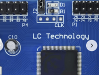
Here is CLK 2, 3, 4 and GND ... External oscillators can be connected here and configured in Quartus - Pin Configuration for relevant pins from schematic ... and reconfigure all pins ... easy - regulator and capacitor can be THT == almost THT solution 🤣
Attachments
Hi,
Has anyone heard significant difference between a shunt PS or a linear one on the digital 5V of AD1862 (or else dac chips) ?
Thanks
Has anyone heard significant difference between a shunt PS or a linear one on the digital 5V of AD1862 (or else dac chips) ?
Thanks
For -18VDC?PSU2 Mini (Minus)
PCB size: 75x25mm
Mouser example -12V:
https://eu.mouser.com/ProjectManager/ProjectDetail.aspx?AccessID=0a78613ee8
200k trimmer from aliexpress: https://aliexpress.com/item/1005001844551366.html
(untested)
R1=270K
R2=12K
R3=400K
R4=2K
TR=200K
For +18VDC?
R1=5k2
R2=330R
R3=30k
R4=2K
TR=50k
Regards,
Dan
Would you please tell us which I/V stage you triedAfter playing for a month with only small bits - different regulators, i/v stages, separate transformers for everything, etc, I still find the high end extension and the soundstage precision lacking. NOS not the main culprit as there is surprisingly little difference between red book and 176kHz.
Passive parts clearly help with the highs, at least to some extent, but i don't believe the soundstage can easily be fixed.
It is perhaps the basic 1862 character. A few decades ago i had a commercial dac with this chip and it was dull as hell. This is so much better.
AD811 at present, original SEN previously.
A couple caveats: AD1862 not on official board but on my 2 layer interpretation. SEN on a proto board.
It is by far the best sounding NOS dac i've had in my system. Previous attempts around Ryan's 1541 D3 topology have not impressed me much (again non official board).
A couple caveats: AD1862 not on official board but on my 2 layer interpretation. SEN on a proto board.
It is by far the best sounding NOS dac i've had in my system. Previous attempts around Ryan's 1541 D3 topology have not impressed me much (again non official board).
Last edited:
@dan
These values are correct. Please note, that maximum allowed input voltage for LT1963 is 20V, better if you do not exceed 19V 🙂
For -18VDC?
R1=270K
R2=12K
R3=400K
R4=2K
TR=200K
For +18VDC?
R1=5k2
R2=330R
R3=30k
R4=2K
TR=50k
Regards,
Dan
These values are correct. Please note, that maximum allowed input voltage for LT1963 is 20V, better if you do not exceed 19V 🙂
Thanks for the heads up. That could've beenThese values are correct. Please note, that maximum allowed input voltage for LT1963 is 20V, better if you do not exceed 19V 🙂
😵 I wonder if I can just squeak by with Power Transformer ?
I'm looking for +/-18VDC for Abraxalito's Dark I/V. I thought your mini PS would be perfect.
Regards,
Dan
AD811 at present, original SEN previously.
A couple caveats: AD1862 not on official board but on my 2 layer interpretation. SEN on a proto board.
It is by far the best sounding NOS dac i've had in my system. Previous attempts around Ryan's 1541 D3 topology have not impressed me much (again non official board).
Curious if you tried opa861, cascoded CEN and also Segios 's Bjt I/V ?
DC coupled or AC coupled ? What, briefly, do you liked more VS the SEN ? I don't want measurements, your words will suffice 😊
For jls usb side I need to drop the voltage to 4. Is there any way to do it with the same 1085 ldo or should I look for a 4V alternative?
- Home
- Source & Line
- Digital Line Level
- DAC AD1862: Almost THT, I2S input, NOS, R-2R
