AD828 or OPA828 ? 😊
In some datasheets, the few stray capacitance can just be messythey write. On some very fast op amp they alert 1 pF of added stray capacitance can make it no stable !😱
It is a good pedagogic input @Joseph K ; indeed better not to play with fast op amps for the ones that like the op amp rolling game w/o adjustments and anyway always uses a resistor at output for prudence...
I layouted the pcbs I made (4 layers but 2 layers as well above in the thread) to try to avoid that added stray capacitance, but I have no iea on how much it contributes to that task... certainly very few stray capacitance as the length of the trace at the input is 5 mm and gnd is removed!) . Well it is certainly only a minor thing in all what one must controls...🤔
Last edited:
yes, unity gain stable opamps are showing the same. For measuring, I shamefully use our scopes in spectrum analysis mode. (Tek, R&S , Lecroy)
Just for illustration, here it is a simulated response: opamp AD828, Rf=20k, load capacity at -In is 0pF, 100pF, 1000pF
Thanks again. Mild peaking like the the one shown in the simulations does not necessarily indicate instability, right? It is perhaps best if it weren't there, but it is also not necessarily a problem.
yes, not necessarily a problem. 🙂Thanks again. Mild peaking like the the one shown in the simulations does not necessarily indicate instability, right? It is perhaps best if it weren't there, but it is also not necessarily a problem.
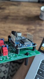
"My JLS came with pre-soldered headers"
This surprised me, because there are different ways users may want to use them.
I have ordered a total of 5 boards on different occasions and they all came with the pins in a tiny packet.
You need to remove them and solder them the other way round, so that the pin can be inserted and sit into the female connectors.
You also need the female connectors on the DAC board.

Not much heat from these resistors, you do not need to leave a gap between resistors and board.Try to get the leads of the resistors fully inserted into the board, allowing the body of the resistors to 'rest' on the board.Started my journey too. Some progress on the DAC side, as well as some PSU work done.
Attachments

Didn't even know the current boards finally have uf.l connectors. Great!
And if you want to experiment with fast op amp with separated buffer,and separate power supply than the 12V for the ad1862 and stilll with uf-l :
there is this one (but LCR tin foil polystyrene not provided as it is smd with a pad large enough to put Rf + Cf ; Basicly : Miro stacked version with outputstage redesigned with independant PS plug for it : https://www.diyaudio.com/community/...st-tht-i2s-input-nos-r-2r.354078/post-7713233
Your welcome.
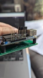
My JLS came with pre-soldered headers.
I can solder a single row of 10 on the H3 side, but H1 is impossible. Is this by design?
I can't believe that. And it has no sense as H3 is a double row mandatory for the I2S cause gnd pins on one row: and JLS knows perfectly that (Lyuben is a very surious guy and very helpfull)
Mine came with just one single row (not soldered of course) and just smd jumper as everybody... I bougth two at 2 years gap, was the same (I just think JLS shoulld provide two jumpers in plus on the H1 pins row)
Hoppefully miro1360 made the first stacked board with the reverse position, but be sure you have this one or if you have the official one it is the further version with the JLS sound not reversed (because the heatsink on it was a problem.)
It is why one has to read the thread to avoid soldering errors and general drawbacks by reading others experience and inputs imho (btw that happen to all of us to make errors)
Second chance is to find a diyer around you genttle enough that has an air flow solder station to desolder the H3 row and H1 row to put both in the rigth position on H3 to have your double row 🙂 . There is hope !😀
EDIT: For the 4 resistors on the miro160, it could makes sense to put 32R up to 100R instead 22R as on the new JLS board the output resistor of the I2S lines are 32R. Don't know if really critical, imho not really (but that 90° knees for fast digital signals maybe a mess, .... dunno)
Last edited:
Or maybe ypu can try to stack it from the bottom but make a slot with a Dremel in the miro board to let the JLS heatsink an area...
It should be possible to remove the plastic from header - either by pulling, heating it up or cutting ... after that you can desolder pins one by one and clean holes with a desoldering pump 🤔My JLS came with pre-soldered headers.
I can solder a single row of 10 on the H3 side, but H1 is impossible. Is this by design?
It may be worth sending a note to Lyuben/JLsounds about this. It would make sense that these were not pre-soldered, which seems to have been the case for most of us.
Thanks, guys, I ll try to remove it. It came together with an oscillator board, maybe this is why.
It came together with an oscillator board, maybe this is why.
If i were you i'd desolder the header off the oscillator board too and invert the sandwich.
It is a problem. oscillator board prevents adding a bigger heatsink therebecause the heatsink on it was a problem.)
- Home
- Source & Line
- Digital Line Level
- DAC AD1862: Almost THT, I2S input, NOS, R-2R