I can’t give any advice here, because сurrent protection in amplifiers for home amateur radio use was stopped installed somewhere in the 90s of the last century, due to its influence on the quality parameters of sound reproduction at high powers, and it was also claimed that it (this protection) increases the noise of the amplifier in the low-frequency range. But I didn’t record these parameters, because I don’t install this protection.To protect against the short circuit, presumably it will be necessary to sense the induced voltage across the 0.22 ohm drain resistors. What max current should the protection circuitry (I'll be using the Hifisonix speaker protection circuit) be set to trip at? Exicon EX10N20/P20 laterals have an Id max of 8A and a max dissipation of 125W
It might sound like a cop out but the Lateral FET's are extremely rugged and failure of them was never ever a worry back in the day. A single pair of the original 7A Hitachi FET's was good for 100wrms/8ohm and nearer 150wrms into 4 ohm as long as the heatsinking was OK. They are immune from thermal runaway in a design like this and they also tend to be 'self limiting' when abused.To protect against the short circuit, presumably it will be necessary to sense the induced voltage across the 0.22 ohm drain resistors. What max current should the protection circuitry (I'll be using the Hifisonix speaker protection circuit) be set to trip at? Exicon EX10N20/P20 laterals have an Id max of 8A and a max dissipation of 125W
Properly designed over current protection should make reference to the SOA (safe operating area) of the device which is a set of graphs determined by both voltage across and current through the FET. The data sheets have these. The protection circuit would include supply rail voltage in the limiting and give a higher current limit for lower supply voltages.
In practice it is just not an issue. I have my rail fuses (per amp) using 3.15AT fuses.

For a CFP type input stage, this is the correct range of the till coil at the amplifier output.
For my education, can you explain why you are calling it a "till coil". I haven't seen that term used for an output inductor. Tried searching but couldn't find anything.
It's actually "Thiele" and is named after the guy who came up with it. The Thiele network (paralleled inductor/resistor in series with the amplifier output to the speaker) is intended to prevent oscillations due to capacitive loads. The Zobel network does the same thing for inductive loads.For my education, can you explain why you are calling it a "till coil". I haven't seen that term used for an output inductor. Tried searching but couldn't find anything.
Right. I normally see it described this way. Or as simply an output inductor. Just curious about the use of the term "till coil".
An inductor is a coil of copper wire, right? overall such a translator))), if I don’t have time to edit, then I end up with such “words”.Just curious about the use of the term "till coil".
came up with ? Then it’s strange, how the mathematician Bouchereau compiled an equation for the inductor. that Thiel “invented” much later. He was the first to actively use it in audio - this yes.It's actually "Thiele" and is named after the guy who came up with it.
It is desirable that this Thiel inductor be wound on a coil in one row, so it will be more linear for audio.
As you say, Neville Thiele was the first to actively use it in audio - "Journal of Audio Engineering" (JAES) 1976 Volume 24 Number 1 pages 20-23. "Load Stabilizing Network for Audio Amplifiers".
Thanks Hennady. I get it now. Language on this site is always an interesting issue with so maybe nationalities and generations represented.
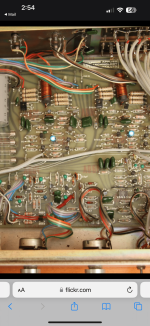
Almost finished now... it's alive and working! Need to tidy up the mains wiring, make a proper front panel and the input wiring with the RCA connectors at the right position (and not just stuck into some existing holes of the recycled case), and then it'll be time to give the amp a thorough listen.
Here's another 'scope shot for power-on. CH1 is the output of one channel, now only peaking up to 5V (nice!). CH2 is the relay voltage; turn-on delay takes 1.3 seconds with my circuit. CH3 and CH4 are the rail voltages, barely 33V with the proper PSU.

And finally some more photos:


Here's another 'scope shot for power-on. CH1 is the output of one channel, now only peaking up to 5V (nice!). CH2 is the relay voltage; turn-on delay takes 1.3 seconds with my circuit. CH3 and CH4 are the rail voltages, barely 33V with the proper PSU.
And finally some more photos:
In the DIY domain " Electronics Australia" magazine offered a project "Playmaster Twin 25" using a Thiele stability network. Thiele was also involved in loudspeaker research where TS parameters are used in design processes. The S is for another researcher surname Small. Since the advent of the Playmaster project Australian Electronics magazines almost invariably include Thiele stability output networks. There was an uprated "Playmaster the Twin 40 published in 1976-1977 so there is a long history of Thiele's stability network being put to practical use for hobbyist amplifier projects.As you say, Neville Thiele was the first to actively use it in audio - "Journal of Audio Engineering" (JAES) 1976 Volume 24 Number 1 pages 20-23. "Load Stabilizing Network for Audio Amplifiers".
A similar inductor was used in "bridge compensation current dumping" that Walker used in the early 70s, but its application was different. Only by examining the parameters of the acoustic system can one understand that there is an equally important applied value of this inductor for amplifiers with a common NFB. Thiel became this engineer, so this is a “Thiel inductor”.Thiele was also involved in loudspeaker research where TS parameters are used in design processes.
I wonder what the inductance of those coils is. They look big enough to have a reasonable value even without a core.
You can use non-air-cored inductors of course, but you'll want to make sure that the core never gets into saturation under normal circumstances. If your inductor starts to saturate at 10A you'll certainly be fine, whereas if it starts to saturate at 2A already, it will introduce distortions that might be audible. It could even be possible that the inductance drops too low for the inductor to be effective with your particular speaker setup and the amp might occasionally break into spurious oscillations.
The main advantage of using a core material at all is that you can build a physically much smaller inductor, and that it can be better shielded by fully encapsulating it into that same material. You might want to look into selecting output filter inductors for Class-D amplifiers, as the problem is exactly the same there. Here is an example for a dual inductor in a single package. They are magnetically shielded from each other, as to not introduce cross-coupling.
Meanwhile my amplifier is now set up in the living room, driving a pair of Infinity's. First impression is superb! 👍
Meanwhile my amplifier is now set up in the living room, driving a pair of Infinity's. First impression is superb!
Well that is the news that we like to hear 🙂
Having thought about how components are steadily becoming available in surface mount options, I took a look at doing a layout to take that into account, this excluding the highest power resistors, the MOSFETS and the electrolytics. I've taken Prasi's excellent dual pair board as the model. Attached is my first take on this and I invite comments on it. Bear in mind it's a learning curve for me with using Kicad 8 for power circuitry.
Attachments
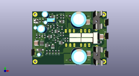
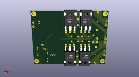
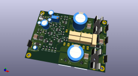
For the mosfet source resistors there's 5W smd resistors from vishay - https://www.vishay.com/en/product/31059/
Datasheet - https://www.vishay.com/docs/31059/wsrhighpower.pdf
There's a 3D model for kicad.
The resistors are available from Mouser, Digikey and Farnell
You should place the mosfet gate resistors as close to the mosfet gate pin as possible, to prevent oscillations.
Datasheet - https://www.vishay.com/docs/31059/wsrhighpower.pdf
There's a 3D model for kicad.
The resistors are available from Mouser, Digikey and Farnell
You should place the mosfet gate resistors as close to the mosfet gate pin as possible, to prevent oscillations.
Last edited:
I think you're going to run into thermal issues with the VAS (Q5) and CCS (Q3) transistors. Based on the simulation files Mooly provided, these dissipate 265mW each. The TO-92 package has a thermal resistance of 83.3C/W for Junction-to-Case and 200C/W for Junction-to-Ambient. This puts the junction temp at 95C. Using the derating figure of 5.0mW/C, the derated power rating is 273mW. These are running right at their thermal limits.
The SOT-23 version of these devices (MMBT5551L/MMBT5401L) has a lower power rating and higher thermal resistance (225 mW and 556 Junction-to-Ambient). Without doing any calcs, we can see that it's well beyond it's thermal capabilities. In addition, these ratings reflect a 25mm x 20mm copper area for heat dissipation, which your layout does not provide.
The other TO-92 devices are likely OK. Their dissipation is less than 20mW.
I'd suggest leaving Q5 and Q3 as TO-92 devices. You could also consider replacing these with KSC3503/KSA1381 if you want to add a bit of safety margin. These seem to work in simulation, though this would be an untested change... proceed with caution.
Thanks for your feedback.For the mosfet source resistors there's 5W smd resistors from vishay - https://www.vishay.com/en/product/31059/
Datasheet - https://www.vishay.com/docs/31059/wsrhighpower.pdf
There's a 3D model for kicad.
The resistors are available from Mouser, Digikey and Farnell
You should place the mosfet gate resistors as close to the mosfet gate pin as possible, to prevent oscillations.
I've had a quick look at the 5W SMD resistors and their footprint appears to be JUST too big to fit in the current locations. I can move the gate resistors with no problem.
I'll take a little while longer to see what else comes back in comments then see what is worth doing.
Thanks for the feedback.I think you're going to run into thermal issues with the VAS (Q5) and CCS (Q3) transistors. Based on the simulation files Mooly provided, these dissipate 265mW each. The TO-92 package has a thermal resistance of 83.3C/W for Junction-to-Case and 200C/W for Junction-to-Ambient. This puts the junction temp at 95C. Using the derating figure of 5.0mW/C, the derated power rating is 273mW. These are running right at their thermal limits.
The SOT-23 version of these devices (MMBT5551L/MMBT5401L) has a lower power rating and higher thermal resistance (225 mW and 556 Junction-to-Ambient). Without doing any calcs, we can see that it's well beyond it's thermal capabilities. In addition, these ratings reflect a 25mm x 20mm copper area for heat dissipation, which your layout does not provide.
The other TO-92 devices are likely OK. Their dissipation is less than 20mW.
I'd suggest leaving Q5 and Q3 as TO-92 devices. You could also consider replacing these with KSC3503/KSA1381 if you want to add a bit of safety margin. These seem to work in simulation, though this would be an untested change... proceed with caution.
I've done the layout using SOT-89 devices, ZXTP5401ZTA which is rated at 1.2W with derating of 9.6mW/degC. and ZXT5551-13 which is rated at 750mW with derating of 166 degC/W. As you say and Mooly's simulation file agree, the VAS (Q5) and CCS (Q3) are the only ones being pushed for power. I'll run my slide rule (spreadsheet really 😉) over these two and adjust / amend as necessary.
- Home
- Amplifiers
- Solid State
- My MOSFET amplifier designed for music