
Looking pretty good!
Flux is your friend. Something like this is extremely useful and will last a very long time. - https://www.amazon.com/dp/B0CH6LBTK4?_encoding=UTF8&psc=1&ref_=cm_sw_r_cp_ud_dp_NXJN40WZQFMCGPPBANE4
Flux is your friend. Something like this is extremely useful and will last a very long time. - https://www.amazon.com/dp/B0CH6LBTK4?_encoding=UTF8&psc=1&ref_=cm_sw_r_cp_ud_dp_NXJN40WZQFMCGPPBANE4
Here some results of testing the P3 with mostly the value parts from the build document. With the same bench power supply as before. The Jfets are changed from 2SK170's to 2SK209'S
With the 2SK209 the Gain is reduced by about 0.8dB. At 0.005 V input the output is 1.52Vrms.
The noise is about the same.
2nd HD is a fair amount greater than with the 2SK170's
3rd HD is noted above the noise floor.
See the attached FFT's for 2SK170's and 2SK209's
Thanks DT


With the 2SK209 the Gain is reduced by about 0.8dB. At 0.005 V input the output is 1.52Vrms.
The noise is about the same.
2nd HD is a fair amount greater than with the 2SK170's
3rd HD is noted above the noise floor.
See the attached FFT's for 2SK170's and 2SK209's
Thanks DT
50 db higher second harmonic with the 2SK209 is rather strange. ??
@DualTriode
Are those genuine K209? I can’t make out any of the markings on the transistor. (Yes, it could merely be the photo)

For reference, they should have “ X G “ on the body -

Are those genuine K209? I can’t make out any of the markings on the transistor. (Yes, it could merely be the photo)
For reference, they should have “ X G “ on the body -
50 db higher second harmonic with the 2SK209 is rather strange. ??
Are those genuine K209? I can’t make out any of the markings on the transistor. (Yes, it could merely be the photo)
What I know about The Jfets is that they came from the vendor on this post:
Pearl 3 Burning Amp 2023
Yes 50dB is a lot.I got out out a magnifier and took a look. The Jfets on the adaptors do have the same X G markings as shown in your photo.
I have a reel of real 2SK209 From Mouser and some little adaptor PCB's. I will solder the known to be real 2SK209's to the adaptors and test them again and see what we get the second time.
Thanks DT
I've dealt with some fake BF862's before. I might have posted about it here a while back.
What I learned following that experience is that fakes are usually re-marked cheap parts. This leaves some telltale signs. The top is usually sanded off to remove the original marking (this leaves sharp edges around the top corners, rather than a slightly radiused original corners), and/or they are painted with some black material to cover the original (the edges of the paint layer can be visible under a microscope). Painted tops may dissolve away with acetone, staining a cotton swab. Sometimes, the font or dimensional tolerances of the markings can be a giveaway, if you know the genuine parts always have consistent markings (some manufacturers use more than one packaging house, so they aren't always identical).
If you're willing to sacrifice a couple of parts, you can take a small blowtorch and burn the plastic package material to a crusty ash, which crumbles off easily. Do that with a suspect and a known genuine part, and compare the die under a microscope.
Here some results of testing the P3 with mostly the value parts from the build document. With the same bench power supply as before. The Jfets are changed from 2SK170's to 2SK209'S
With the 2SK209 the Gain is reduced by about 0.8dB. At 0.005 V input the output is 1.52Vrms.
The noise is about the same.
2nd HD is a fair amount greater than with the 2SK170's
3rd HD is noted above the noise floor.
See the attached FFT's for 2SK170's and 2SK209's
Thanks DT
View attachment 1281493View attachment 1281494
-UGS
What's up with the VGS?
Do you have the gate-source voltage ready for comparison? Comparing to the k170BL and the k209GR type on your board?
I have a suspicions, but ultimately it's strange ...
I'd go over the solder joints of your bare copper CAT6 wires to those PCB's, with flux this time. The Gate and Source joints of the PCB on the far right look particularly cold and dry. 'Might just be a bad pic - 'sorry if that's all it is....little adaptor PCB's...
Not too difficult to catch bogus LN JFETs. Temporarily disable C3 by unsoldering one leg. Place 390R in parallel with the 47k input resistor resistor.
With an insulated tweezer place the JFET on the SMT pads and power up. Run an FFT and spot the voltage at 1kHz -- should be around 2.5nV/RtHz (after you divide by the gain of ~22 for a single JFET). Remember to adjust your bins.
With an insulated tweezer place the JFET on the SMT pads and power up. Run an FFT and spot the voltage at 1kHz -- should be around 2.5nV/RtHz (after you divide by the gain of ~22 for a single JFET). Remember to adjust your bins.
the back side of the joint is show. it looked good from the other side.I'd go over the solder joints of your bare copper CAT6 wires to those PCB's, with flux this time. The Gate and Source joints of the PCB on the far right look particularly cold and dry. 'Might just be a bad pic - 'sorry if that's all it is.
View attachment 1281607
I did reflow the solder prior to plugging in the little buggers into the sockets.
How can it be explained that distortion is so much higher with 209 vs. 170?
Since 5 mV input gives 1.5 V out the gain is set to MM (low).
Could it be that the 170 input circuit better likes the "high" input signal from a MM cartridge?
Maybe most tests have been made using the high gain settings with low input signal (MC signal)?
I am just guessing........but I am happy so far that I used 170 in my build and I use MM 5 mV output cartridge 🙂
One more question:
Which R1 resistor do you use? .....do you change it for 209 vs. 170.
I am thinking about if Q5 is saturated or not or maybe saturated when using 170 and not using 209 etc.?
It could make sense that the higher bias in 170 input circuit handles better high input voltage or.......?
I was able to complete the Pearl3 boards today. Thank you to all for your sharing of pics and results. Getting close to live testing.
Using the kit supplied parts, the 2SK209s came in within +/-0.2mA in circuit running an average of 1.9mA each. Q5 is running C-E voltage 1.9Vdc to 2.1Vdc.
The 2SK170s ran much more current, around 4.7mA each. That put Q5 into saturation with C-E voltage a little under 0.2Vdc.
NOTE: Boards tested with a load resistor on the input and using the kit provided PS one board at a time.
Outputs had around 0.2mV of AC noise. Not bad with boards open, sitting on a desk next to a computer, cell phone and in the same room as my wireless router. 🙂
Hello All.
Today I replaced I replaced the Jfets with 2SK209 GR. The Jfets are direct off a reel purchased from Mouser a year or so ago. They are known to be the real thing.
The voltage across R1 measured 6.79Volts with 9.05 ma. At 5ma input the gain is 42.54dB and THD+N is 0.462%
The noise floor is higher perhaps 1/f noise. The 2nd HD remains higher than the 2SK170
The steel J box (cookie tin) does a good job of reducing power supply harmonic noise.
See the FFT below.
I do not know the story about the elevated 2nd HD.
Thoughts?
Thanks DT
How can it be explained that distortion is so much higher with 209 vs. 170?
Since 5 mV input gives 1.5 V out the gain is set to MM (low).
Could it be that the 170 input circuit better likes the "high" input signal from a MM cartridge?
Maybe most tests have been made using the high gain settings with low input signal (MC signal)?
I am just guessing........but I am happy so far that I used 170 in my build and I use MM 5 mV output cartridge 🙂
One more question:
Which R1 resistor do you use? .....do you change it for 209 vs. 170.
I am thinking about if Q5 is saturated or not or maybe saturated when using 170 and not using 209 etc.?
It could make sense that the higher bias in 170 input circuit handles better high input voltage or.......?
R1 is 750R for both.
Bias for 170's was 12ma total
Bias for 209's was ~10ma total
Ok, most seems to have about 12 mA for the 170 BLs but much less than 10 mA for the 209 GR's?
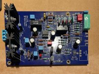
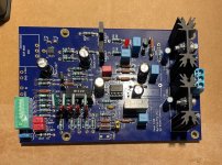
Looks good! Great job!A picture of each board. The SMD parts were a challenge. Again, tips from the forum made the difference for me. Thanks guys!
Glad to hear it; hope you are not offended by my comment.it looked good from the other side.
So with the 2sk170, Q5 is well into saturation; with the 2sk209, Q5 is on the verge.
Are you interested in seeing what happens if Q5 is not "on the verge". Other than juggling R1, Wayne had recently suggested in #2554 reducing R3.
...A different strategy with regards to the cascode is to make R3 4.75K...
- Home
- Amplifiers
- Pass Labs
- Pearl 3 Burning Amp 2023