I saw something close to the first picture. But i will go up to 10khz ir even 18-20khz and see it in action. I think i will be able to reproduce this result you show here woth zero bias.Pretty much anything will work in practice 😉 the 5550 and 5401 are great default and they never blow up (in a sim) even at several kW dissipation.
@alexpriftis85
You mentioned crossover distortion earlier. Here is the amp with zero bias at 1kHz and then 10kHz. The distortion is just visible in the first image but obvious at the higher frequency.
View attachment 1219126
View attachment 1219127
I didn't even think about going above 1khz. I thought that if i had crossover distortion it would be on the full spectrum.
If you try it you will only see the distortion with a load attached.I saw something close to the first picture. But i will go up to 10khz ir even 18-20khz and see it in action. I think i will be able to reproduce this result you show here woth zero bias.
When testing at higher frequencies keep the level low because higher frequencies are where the Zobel network comes into play and it is common for the resistor to be under rated for continuous sine testing at high power. Those are the 0.1uF and 10 ohm at the output on my sim. I'm assuming your amp has those but your diagram didn't quite show that far to the right 🙂
In any case crossover distortion shows best at lower levels. 4 volts peak equates to 1 watt into 8 ohms and that is fine, just don't crank it up to full output.
I'll look in again tomorrow.

When i used the oscilloscope and posted the pictures a couple pages back in this thread i had a regular 2-way 60w speaker connected as a load. I don't have dummy loads so my ears kinda got stressed with this 1khz sine wave at 50% power 😅😅😅If you try it you will only see the distortion with a load attached.
When testing at higher frequencies keep the level low because higher frequencies are where the Zobel network comes into play and it is common for the resistor to be under rated for continuous sine testing at high power. Those are the 0.1uF and 10 ohm at the output on my sim. I'm assuming your amp has those but your diagram didn't quite show that far to the right 🙂
In any case crossover distortion shows best at lower levels. 4 volts peak equates to 1 watt into 8 ohms and that is fine, just don't crank it up to full output.
I'll look in again tomorrow.
I will test with low volume high frequency on the speaker again and "zoom in" on the oscilloscope. 😊
Stop using a speaker as load!
You risk your speaker.
Buy some 16 ohm/17w power resistors.
Connect two parallel and you will have an 8 ohm dummy load.
Speaking for pictures that you have posted,are those pictures before output replacement?
You risk your speaker.
Buy some 16 ohm/17w power resistors.
Connect two parallel and you will have an 8 ohm dummy load.
Speaking for pictures that you have posted,are those pictures before output replacement?
I know i shouldn't but i had to test it somehow hahhaha.
It's a "sacrificial" speaker if anything goes wrong. But yes i plan to do that anyway (buy resistors for dummy load)
Also the previous times the amp blew it was connected to actual speakers as i thought it was fixed and had it playing on my working desk for days.
Each and everytime the relay/protection circuit saved the speakers thankfully.
Right now it won't be connected to any speaker until i perform more tests and measurements. I will also be on the dim bulb during those tests so that i minimize the damage should anything go very wrong.
I'm going to say if you use a speaker as a load to see crossover distortion then turn the level down from your 50% to something closer to 99.8% lower (really). Try it at around 0.1 volts peak output.
Can you explain further how i will test the transistor and see if it survives? I did not quite understand that one. i do have a bench power supply 0-30v 2.5ampsYou need TO264 case style.
No,i don't suggest you the test gear to match but to see if transistor under test will survive.
Do you have a functional chanel now?
Also i found that the "o" type of 2sc5200-O and 2sa1943-O are available on mouser. Should i order them? Also since they are bigger i will need bigger insulation pads. The tape on the cooling block has started to degrade. The call them "Mikas. What size should i get for those transistors?
You'll need these 'Mikas' called sil-pad. No need to apply any grease.
https://www.mouser.be/ProductDetail/Bergquist-Company/SP400-0.007-00-104?qs=jQRjkUoUCJcSyLJh2yRkNg==
For the small bias transistor in between the big outputs, i'd use the same but cut them to size.
I always check for conductivity between the collector and ground to make sure the insulation is OK.
If that fails, in your case that would connect the + or - 56V to ground, which you don't want.
Hugo
I've been doing some reading on the transistors, biasing, breakdown voltages etc. So that i can understand better what conditions that should be present in order for the output transistors to fail.
I was looking at breakdown voltages especially and the max current of the 2sa1941 and 2sc5198 both are the same with the expeption of positive and negative values. Lets take as an example the 2sa1941 datasheet here: https://datasheetspdf.com/pdf-file/701460/InchangeSemiconductor/2SA1941/1

So in theory in order for this to fail:
- Voltage between base and collector should be over -140v
On the marantz i have -56v on the collector and a few milivolts at the base (dc voltage present due to idle current biasing right?). And even if i had let's say +56v on the base for any reason i would still be lower than the 140v. But i would have excessive current and still fry the transistor right?
- I'm guessing the same principle applies for the rest of the readings in order to fry the transistor:
Voltage across collector - emitter > 140v OR voltage across base - emitter > 5v
-As far as current is concerned:
i need over 1A at the base to fry it and over 10A coming out of the emitter from collector in order to fry it. Right?
Mooly mentioned and showed that even a 0.1volt could increase how a transistor conducts up to 35%!
So i cannot understand in the specific amplifier design how could i possibly get over 1A at the base or over 140v / 5v.
Even if i shorted the positive and negative rails i would not reach that kind of number in voltages.
Even with biasing at maximum i don't think i could get it to reach over 1A of continuous current with the voltages i'm generaly seeing on the circuit from the emitters of the drivers and predrivers all the way up to the outputs. So.. These transistors are amplifying current and this translates to higher voltages am i correct so far?
Have i understood the theory correctly?
And if the transistors are fake then the breakdown voltage or the the maximum current at their bases is much lower than what the datasheet states. So when i bias them they fail. Correct? And a different failure mode is the actual breakdown voltage that is lower thatn the 56v volts applied from the power supply causing them to also breakdown and conduct uncontrollably.
I was looking at breakdown voltages especially and the max current of the 2sa1941 and 2sc5198 both are the same with the expeption of positive and negative values. Lets take as an example the 2sa1941 datasheet here: https://datasheetspdf.com/pdf-file/701460/InchangeSemiconductor/2SA1941/1
So in theory in order for this to fail:
- Voltage between base and collector should be over -140v
On the marantz i have -56v on the collector and a few milivolts at the base (dc voltage present due to idle current biasing right?). And even if i had let's say +56v on the base for any reason i would still be lower than the 140v. But i would have excessive current and still fry the transistor right?
- I'm guessing the same principle applies for the rest of the readings in order to fry the transistor:
Voltage across collector - emitter > 140v OR voltage across base - emitter > 5v
-As far as current is concerned:
i need over 1A at the base to fry it and over 10A coming out of the emitter from collector in order to fry it. Right?
Mooly mentioned and showed that even a 0.1volt could increase how a transistor conducts up to 35%!
So i cannot understand in the specific amplifier design how could i possibly get over 1A at the base or over 140v / 5v.
Even if i shorted the positive and negative rails i would not reach that kind of number in voltages.
Even with biasing at maximum i don't think i could get it to reach over 1A of continuous current with the voltages i'm generaly seeing on the circuit from the emitters of the drivers and predrivers all the way up to the outputs. So.. These transistors are amplifying current and this translates to higher voltages am i correct so far?
Have i understood the theory correctly?
And if the transistors are fake then the breakdown voltage or the the maximum current at their bases is much lower than what the datasheet states. So when i bias them they fail. Correct? And a different failure mode is the actual breakdown voltage that is lower thatn the 56v volts applied from the power supply causing them to also breakdown and conduct uncontrollably.
The devil is in the detail.Have i understood the theory correctly?
You need to look also at max power dissipation. Power is current multiplied by voltage and so you should never have a combination of I and V that will cause the power rating to be exceeded. A 140 volt rated transistor with a max power dissipation of 100 watt and max current rating of 10 amp can only pass 2 amps if there is 50 volts across it before its rating is exceeded.
It also gets a bit more complex than that because of something called secondary breakdown.
https://en.wikipedia.org/wiki/Safe_operating_area
I think you will find the vbeo figure is under reverse bias conditions. When forward biased the junction behaves much like a diode and you will not see much more than lets say 0.8 volts between base and emitter, even under high current conditions. When the base/emitter is reverse biased the transistor turns off but at around 5 to 7 volts the junction begins to conduct and that could be destructive.
Years and years ago operating the base/emitter junction of a small transistor at low current was a way to generate white noise. As long as the current is limited the junction is safe.
An amp like the Marantz and all analogue circuitry really will never place a transistor in that reverse biased state.
Here is your amp delivering 28 volts rms into 8 ohm (100 watts).

And I've just done a quick switch of the output transistors to something more representative, the MJL21194 and 21193. Nothing else changes.
This shows the base current of the output transistors at around 100ma peak. The peak load current is 5 amp and so very very approximately the gain of these simulated transistors is 5/0.1 which is 50.

Now I'll swap just the upper NPN to a 2N3055. The gain is much lower and base current much higher for the NPN. The output signal is unchanged though thanks to the action of the negative feedback loop.

And I've just done a quick switch of the output transistors to something more representative, the MJL21194 and 21193. Nothing else changes.
This shows the base current of the output transistors at around 100ma peak. The peak load current is 5 amp and so very very approximately the gain of these simulated transistors is 5/0.1 which is 50.
Now I'll swap just the upper NPN to a 2N3055. The gain is much lower and base current much higher for the NPN. The output signal is unchanged though thanks to the action of the negative feedback loop.
So many details... In your example i can understand that the feedback loop brings the output to a balance even though the transistors are very inbalanced and the base current is totally different. In this phase i'm trying to learn failure modes on the transistors, common faults and use this amplifier design and my problem to put the theory to the test.
I'm curious what values am i going to see on each stage once i change that 270ohm resistor to a 220 ohm and max out the bias on the trimmer (while on the dimbulb). I want to see the actual behaviour on each stage as the current increases with this technique. And understand if those transistors are fake indeed. If they are they will break down quite fast assuming i have the time to measure everything before that happens.
I'm curious what values am i going to see on each stage once i change that 270ohm resistor to a 220 ohm and max out the bias on the trimmer (while on the dimbulb). I want to see the actual behaviour on each stage as the current increases with this technique. And understand if those transistors are fake indeed. If they are they will break down quite fast assuming i have the time to measure everything before that happens.
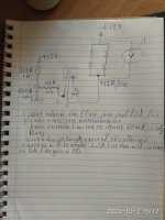
Here is a symlified test gear suitable for power transistor measurements.
Screw the power transistor in a big heatsink.
Reverce the supply polarity for PNP devices
Screw the power transistor in a big heatsink.
Reverce the supply polarity for PNP devices
Attachments
Last edited:
Here is a symlified test gear suitable for power transistor measurements.
Screw the power transistor in a big heatsink.
Reverce the supply polarity for PNP devices
Thank you! that is much simpler and do-able! So to make sure i understand this correctly:
- I measure voltage on those 4 resistors at the end ( upper right in the photo // they connect to the collector ). So this is my supply voltage to the transistor (56 volts on the actual amplifier circuit or -56v for the PNP)
- There is another supply voltage 12v and goes to the base of the transistor through a trimmer with 100 ohm range and a static resistor of 100ohms to set the bias. correct?
- Emitter goes to ground (for the NPN for the PNP i will be +12v )
Ok so now what? let's say i adjust the trimmer and what do i measure? You show a voltmeter on the collector on those resistors. What should i be seeing and testing?
Although transistors can fail many different ways a quick summary is that power transistors such as the outputs tend to fail short circuit from C to E.In this phase i'm trying to learn failure modes on the transistors, common faults and use this amplifier design and my problem to put the theory to the test.
Smaller driver transistors also typically fail in this way although they can also become leaky meaning they conduct when they should be off. That typically shows as a reading other than open circuit when biased in the correct way with your meter. Remember for a DVM the red lead is the one with a positive test voltage on it relative to the black lead. So for a NPN device you place the red lead on the collector and black on the emitter. There should be no conduction on any range although if your meter has a really high ohms range you might see a reading of a few meg ohms. Leakage is typically in the hundreds of ohms or a few k ohms.
Transistors that are suspected of intermittent faults are often those that run permanently hot in a circuit and typically show an anomaly in the base/emitter voltage with that suddenly rising above the expected 0.6 to 0.7 volts when the fault occurs.
Try the simulation 🙂I'm curious what values am i going to see on each stage once i change that 270ohm resistor to a 220 ohm and max out the bias on the trimmer (while on the dimbulb). I want to see the actual behaviour on each stage as the current increases with this technique.
Here is the output stage at 40 milliamps bias, 1 amp bias and then zero bias.
It is very difficult to test and prove if a power transistor is a fake. You can get clues by checking the breakdown voltage but you need a power supply capable of exceeding the expected values. Another good test is to look at the gain at high frequency and see how it compares to a known original part. Also checking just the DC current gain can be useful but ultimately it is very very difficult to say for sure without quite involved testing.And understand if those transistors are fake indeed. If they are they will break down quite fast assuming i have the time to measure everything before that happens.
No,you need only one 12v/5A power supply.
The same power supply for collector and base.
The volmeter across collector resistors is for voltage measurement .
Then you can calculate the collector current.
I=V/R.
I didn't test myself if a fake one can survive at 2A continues for about 30'.
I can test this as i have some NJW0281 for shure fake.
Last edited:
Ok! Got it! Thank you!!!No,you need only one 12v/5A power supply.
The same power for collector and base.
The volmeter across collector resistors is for voltage measurement .
Then you can calculate the collector current.
I=V/R.
Try the simulation 🙂
Here is the output stage at 40 milliamps bias, 1 amp bias and then zero bias.
In this simulation even with no bias current i see an almost perfect symmetry between the positive and negative values in all 3 cases. And i mention this because in my case the negative side is wayyy lower. BUT you showed me an example earlier today where you replaced one of the two transistors in the output and the feedback circuit balanced them.
So in essence with higher bias i will see higher voltage values all the way up to the final transistors and despite them being different the feedback loop will cause the output signal to be symmetrical.
I installed LTspice, added the junction that you said you were missing and run a few tests altering the trimmer value and the 270ohm resistor (in your schematic you have it 235). Very interesting indeed! i love it! The only thing i could not get to simulate is the waveform you showed on previous pictures.
My only indicator at this point that those are clones/fake is that these transistors fail:It is very difficult to test and prove if a power transistor is a fake. You can get clues by checking the breakdown voltage but you need a power supply capable of exceeding the expected values. Another good test is to look at the gain at high frequency and see how it compares to a known original part. Also checking just the DC current gain can be useful but ultimately it is very very difficult to say for sure without quite involved testing.
- Without proof of overbiasing / excessive current. At all previous repairs when they failed the bias was either zero or i had a low idle current reading on the emitter resistors (0.18 ohms)
- The power supply kept a solid +-56v without fluctuating
- The transitors where cool when they failed (to me this is another proof that no continuous excessive current was drawn from the transistors they where not fully on all the time)
- No oscillation detected and no feedback loop failure detected (checked with oscilliscope and checked feedback loop components on both channels)
- Dc offset was stable at 20-30mv depending on the channel with no fluctuations
So at this point my only guess is that those transistors could be fake and don't have the expected specs so they blow up when they are biased or they are close to being biased or there is a voltage breakdown happening instantly (explains the rapid shorting of the transistors while they are cool)
That's why i expect for them to maybe survive on the dimbulb when i get them to bias by changing that 270ohm resistor you suggested to a lower value, but to be hinest i expect them to blow almost in 5 minutes if i try to bias them wihtout the dim bulb.
And the 3rd option is:
let's say they survive without the dimbulb and get them biased properly, the amp will play for a few hours and then boom blow up again.
At least that's what has been happening so far. So yeah i strongly tend to believe those are fake with wrong specs after almost a month of troubleshooting and since i have replaced about 32 (!!!) of them already from the same supplier thinking i was doing something wrong or missed something.
Last edited:
Higher bias means all the transistors have to conduct a bit more and that is reflected in the slightly higher base/emitter voltages. Remember the transistors are really current driven and the base current is higher for increased bias current.So in essence with higher bias i will see higher voltage values all the way up to the final transistors and despite them being different the feedback loop will cause the output signal to be symmetrical.
At zero bias the output transistors are fully off (and there is no voltage across the b/e junction). When a signal is applied the negative feedback attempts to swing the output across this 'dead zone' extremely quickly and the result is that you still see an almost perfect output despite the fact the unbiased output transistors are 'blind' and non conducting in that -0.6 to +0.6 volts zone.
The only way you will prove this is to be sure the devices you fit are genuine. They don't automatically have to be the same type as you can often substitute parts, particularly when originals are hard to come by or expensive but you must always ensure that what you fit is a genuine part whether that is original or a substitution.At least that's what has been happening so far. So yeah i strongly tend to believe those are fake with wrong specs
It is an even simpler method to test but this requires another good working amplifier.
A diy amplifier is fine.
Fit your Power pairs to this and stress it!
Simple.
A diy amplifier is fine.
Fit your Power pairs to this and stress it!
Simple.
Ok now we are getting somewhere!!!
- i replaced the 270ohm resistor (R3302) with a 220 ohm resistor and installed the new multiturn 100 ohm pot.
- i can now adjust bias while on the dim bulb!!! Wow Professor Mooly was right again!
-i have it iddling for 20 minutes now while on the dim bulb with 14-15mv of idle current at first and now that it warms up it has dropped to 12.6
I would expect it to go up not down as it warms up but im on the dim bulb maybe that's affecting things.
No explosions yet BUT the dim bulb is brighter here are 2 pics :
- Home
- Amplifiers
- Solid State
- Marantz PM-68 Keeps Frying Output Transistors on Right Channel