What is this 1ma?I assumed 1mA bias needed by the amp, plus 5mA bias into the Zener, total 6mA. Assuming 20V across the resistor, 20V/6mA=~3.3K
Baldin elected a bit lower current in the Zener. Either should be fine and not produce so much destructive heat.
20V across 680 = 0.59W in the resistor and about 0.34W in the Zener
I am planning to run it with 3.7M/0.22 r6 and r30 combination. With my current 36.6v power rail. it gave about 900ma quiescent current, using two fans inside to cool, is that too crazy?
Simulation shows in this setup, for 680ohm r13, the current through it is 35.5ma, and 855mw power dissipation.
Change it to 3.3k will get 7.4ma current through and 180mw power dissipation. Meanwhile quiescent current through r30 will be 886ma, that sounds better way to go

re: #141
The transformer only delivers its rated voltage at its max. rated load. Small transformers including the original toroidal types, have the poorest regulation, which is to say that under load, their DC supply voltages could sag by some 7-10% of their unloaded voltage. If you were to disconnect the DC power to either or both amplifiers thus removing their bias current load, you'd see this in action when you compared the DC voltages in each case.
The transformer only delivers its rated voltage at its max. rated load. Small transformers including the original toroidal types, have the poorest regulation, which is to say that under load, their DC supply voltages could sag by some 7-10% of their unloaded voltage. If you were to disconnect the DC power to either or both amplifiers thus removing their bias current load, you'd see this in action when you compared the DC voltages in each case.
Last edited:
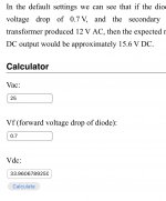
are u saying I should have got lower voltage? but in fact I am getting 36.6v, with bulb removed, which is a bit higher than I expected.The transformer only delivers its rated voltage at its max. rated load. Small transformers, including the original toroidal types, have the poorest regulation, which is to say that under load, their DC supply voltages could sag by some 7-10% of their unloaded voltage. If you were to disconnect the DC power to either or both amplifiers, thus removing their bias current load, you'd see this in action when you compared the DC voltages in each case.
Just in case anyone interested.
following up previous quiescent current measurement:
880ma for 3.7M*0.22
442ma for 3.7M*0.47
777ma for 1.8M*0.47
1.5a for 1.8M*0.22
204ma for 16M*0.47
here I attached the 1khz sinewave frequency response of different settings from above, simulated in LTspice,
thanks to Baldin providing me the simulation file.
Attachments
Think about it. It means you will have a higher than normal voltage if the load is less than normal. If for example, you were to disconnect one of the amplifiers or the bias current was low for some reason, you have reduced the load and should expect a higher voltage supply to the remaining one.are u saying I should have got lower voltage? but in fact I am getting 36.6v, with bulb removed, which is a bit higher than I expected.
Also, check the AC voltage direct from the transformer windings - it should almost track (less diode voltage drop) with the rectified DC output.
Last edited:
with 120va transformer, 25-0-25 AC, after rectifier, 36.6-0-36.6 DC, what value of quiescent current is realistic? maybe 900ma is too high for this voltage?
I am not sure how to calculate.
I am not sure how to calculate.
hum... i've been following along if ZD1 and R13 are running hot but everything in the pre-amp stages of this amp is fine, then that would suggest to me to C8 is bad... trying subbing it and see how things run then...i venture your bias upset will go away!
otherwise your back to pcb problems...to that, when you say you checked for that what was your multimeter setting?
otherwise your back to pcb problems...to that, when you say you checked for that what was your multimeter setting?
Sorry, the 1mA I was referring is controlled by the current through R5 and R12, about 1mA. This is the only current drown from the Zener regulators. Trying to emphasize the unnecessarily large Zener bias and dissipation given the small requirement. A lot of widespread damage and grief for no reason.What is this 1ma?
I am planning to run it with 3.7M/0.22 r6 and r30 combination. With my current 36.6v power rail. it gave about 900ma quiescent current, using two fans inside to cool, is that too crazy?
Simulation shows in this setup, for 680ohm r13, the current through it is 35.5ma, and 855mw power dissipation.
Change it to 3.3k will get 7.4ma current through and 180mw power dissipation. Meanwhile quiescent current through r30 will be 886ma, that sounds better way to go
If I understand your question, there's no equation that sets the "best" current. It's a judgement call, a tradeoff between dissipation and whatever merits you believe come from Class A mode.with 120va transformer, 25-0-25 AC, after rectifier, 36.6-0-36.6 DC, what value of quiescent current is realistic? maybe 900ma is too high for this voltage?
I am not sure how to calculate.
Last edited:
The fact that you see improvement after the carving effort is confirmation that suspicions re carbon have been correct, IMO. But the fact that TR1 base is still negative indicates that carbon leakage remains a problem.Of course its been checked, not conductive, all obvious suspicions have been checked.
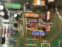
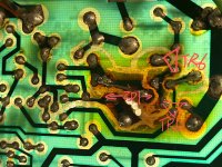
As people suggested, I carved the burned area as much as I can without completely remove and rebuild it. See pictures attached.
It seems improved a bit after that work, I am not 100% sure.
Now tr1 and tr2 emitter are around 480-500mv, about 100mv below ideal case.
Tr1 base still negative around -60mv, thats about 90mv below expected.
R15 is around -3.5v, thats about 1v below expected.
Rail voltage increased to 20v, with bulb attached.
The picture showing the carved paths is very helpful. Would you mark on a schematic an indication of where these carved tracks are relative to the components and adjacent circuit tracks? I'm trying to understand exactly where TR1/2 bases are within the burned regions and carved trenches.
Thanks.
There are two limits, heat and the transformer power.If I understand your question, there's no equation that sets the "best" current. It's a judgement call, a tradeoff between dissipation and whatever merits you believe come from Class A mode.
in the current setup, heat mainly comes from ZDs, R13, r19, exactly where the burn marks are. This is due to raised rail voltage from A1’s 20v rail to MA50’s 32v+ rail. This can be resolved by increased r13 resistor value and use higher power resistor, not too big a problem.
that left the transformer power, I was trying to copy combinations from A1s (there are many different A1 versions, with r6,r30 combinations I listed above). Then I realised, due to the fact I have 36.6v rail voltage comparing to A1 20v, the power could be much bigger than A1 if I use the same A1 setup.
In the simulation it shows with about 900ma quiescent current, tr9/10 are running at 35+watts each, almost doubled comparing to 20v rail. So I am working if I running out of transformer power in this case, because there are 4 output transformer inside, these alone will consume more than 120w standby by in class A mode.
I can see potential problem through simulation, but not sure exactly how to do the math, that’s why I asked.
Instinct tells me that peak currents will be higher near clipping than the Class A current. If the supply can deliver the peak currents, it can deliver the quiescent current. Dissipating power is a separate consideration.
This amp certainly has an interesting design.
As has been noted somewhere, the amp features two feedback paths, namely R25,R23,C14 and R24,R22,C13. I believe mismatch between these two paths is a distortion mechanism. For simplicity, if we assume pure Class B operation, positive half-cycles are controlled by R25,etc and negativehalf-cycles are controlled by R24,etc. I believe a 1% mismatch in the feedback ratios yields 0.5% distortion. Consequently, I recommend these four resistors have 0.1% tolerance. A further consideration is the ESR of the capacitors: 0.1% of R23 is 2.7 ohms, so the ESR of C14 should be small relative to 2.7 ohms. eg https://www.digikey.com/en/products/detail/kemet/ESY476M025AC3EA/3083078
As has been noted somewhere, the amp features two feedback paths, namely R25,R23,C14 and R24,R22,C13. I believe mismatch between these two paths is a distortion mechanism. For simplicity, if we assume pure Class B operation, positive half-cycles are controlled by R25,etc and negativehalf-cycles are controlled by R24,etc. I believe a 1% mismatch in the feedback ratios yields 0.5% distortion. Consequently, I recommend these four resistors have 0.1% tolerance. A further consideration is the ESR of the capacitors: 0.1% of R23 is 2.7 ohms, so the ESR of C14 should be small relative to 2.7 ohms. eg https://www.digikey.com/en/products/detail/kemet/ESY476M025AC3EA/3083078
Replaced c8, nowhum... i've been following along if ZD1 and R13 are running hot but everything in the pre-amp stages of this amp is fine, then that would suggest to me to C8 is bad... trying subbing it and see how things run then...i venture your bias upset will go away!
otherwise your back to pcb problems...to that, when you say you checked for that what was your multimeter setting?
Tr1, tr2 emitter 555mv
Tr1 base: -3mv to -8mv
Tr2 base -14mv to -17mv
R15 -2.9v
Rail voltage 23.8v
There are slight improvement, though I am not quite sure if the improvement is directly related to c8 replacement.
I am not quite sure your question about multimeter setting, I just set to dc voltage test when test dc voltage, diodes mode for transistor test, continuity mode for short/continuity checks. Just normal operation. I got two multimeters, shouldn’t be multimeter problem
C14 and c10 has been replaced with bipolar capacitors yesterday. C10 not yet, as the film capacitor ordered hasn't arrive yet.
Everything I did seems improve it a little bit, including carving the PCB, I am still not sure exactly which one caused it.
C10, and C13 are almost certain caused the problem mentioned in the tiled, the distorted sound. But they look to me are damaged as a result of abnormal voltage, not the cause.
Now the voltage is coming back to normal gradually, tr1 and tr2 base is very close to positive. The long tailed transistor pair and the feedback indeed make things hard to debug.
This amp does have amazing design, I was surprised by how nice they sound as such a minimal design.This amp certainly has an interesting design.
As has been noted somewhere, the amp features two feedback paths, namely R25,R23,C14 and R24,R22,C13. I believe mismatch between these two paths is a distortion mechanism. For simplicity, if we assume pure Class B operation, positive half-cycles are controlled by R25,etc and negativehalf-cycles are controlled by R24,etc. I believe a 1% mismatch in the feedback ratios yields 0.5% distortion. Consequently, I recommend these four resistors have 0.1% tolerance. A further consideration is the ESR of the capacitors: 0.1% of R23 is 2.7 ohms, so the ESR of C14 should be small relative to 2.7 ohms. eg https://www.digikey.com/en/products/detail/kemet/ESY476M025AC3EA/3083078
I actually just bought a bunch of good tolerance resistors to replace all of the old resistors. Including r8, r7, r22, r24 but most of them I bought as 0.5% or 1% tolerance, could have bought 0.1% one for r23 if you mentioned earlier.
C13 and c14 I have replaced are bipolar. But they only comes with 20% tolerance options. That seems quite big.
Maybe its more clear to see from front view as well.The picture showing the carved paths is very helpful. Would you mark on a schematic an indication of where these carved tracks are relative to the components and adjacent circuit tracks? I'm trying to understand exactly where TR1/2 bases are within the burned regions and carved trenches.
Thanks.
The two picture I attached are front and back view. I flipped the back view picture, so it directly maps front view
Attachments
after I did some more carving, reinforced week connections, clean up PCBs.
most of the voltages become normal, even tr1 base is a small positive voltage now.
except now tr9 collector is around 0 mv. tr10 collector is around 100mv.
while on the other channel, tr10 is about 60mv, tr9 is around -60mv.
So I think I still have problem with unbalanced up and down part of the circuit in this channel. Seems when the bottom part is working quite good now, up part circuit and tr10 collector is pulling up the voltage of tr9 collector. That seems to me the up part may also suffer a bit from carbon track problem.
I am actually pretty confident most parts I replaced, are good parts. Except c13 or c10( more likely just c13), which when got replaced, fixed distortion problem.
so as a CONCLUSION:
it is the PCB board carbon tracks caused the problem — wrong Voltage, then wrong voltage caused c13 to negatively charged, hence failed.
I guess there are still some carbon track problem in the up part of the circuit (positive rail), which caused imbalance between positive and negative circuit. I also feel the carbon tracks/contamination is a little bit heat sensitive.
In this circuit, the feedback loop is quite sensitive, carbon track problem makes accurate match of spec almost not possible or too hard to achieve. Using better tolerance rating components to achieve low distortion also become meaningless in this case.
So I doubt whether this PCB is still worthwhile to repair and put expensive components like film caps, bipolar capes, low tolerance resistors on it? For a complete rebuild of this amp, to achieve the design goal performance, a new PCB looks to me is inevitable.
Your continuing experiments seem to add further evidence that you're on the right track. I agree with your conclusions.
I'm not sure how to advise you. You've got a lot of time and effort already invested in this board. I can recall similar experiences; as the board approaches the point of being a hopeless case, it's a bit liberating--- you can attempt bolder measures because there's little left to loose anyway. Success is sometimes the payoff.
Cutting suspicious tracks just beyond the burned areas and then jumpering the severed traces may be easier than trying to thoroughly excavate damaged material (and success more assured). If a lead of a sensitive component lies within a burned region, pull it out of the board and improvise a through-the-air connection. If you eventually get the amp performing as it should, then you can swap in close tolerance parts for better performance. BTW, your caps may already have adequately low leakage--- I didn't know what parts you have chosen.
If you get stuck in a particular, area-top or bottom, I'll try to offer advice.
Good luck!
- Home
- Amplifiers
- Solid State
- Help please, Musical Fidelity A1/MA50 one channel distorted after about 10 seconds