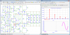
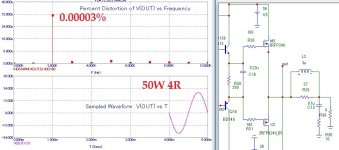
Here you can see the difference between BJT - VMOS final transistors at different quiescent currents and different output voltages.Is this poor THD? This is real measurement on the 200W version.
The reason why I don't prefer VMOS I think is clear.
Attachments

A very clear comparison, and it is also clear that a supply voltage higher than +/-35-36 volts is not desirable for mosfets, and the depth of the overall negative feedback with increasing frequency is needed much more.The reason why I don't prefer VMOS I think is clear.
The supply voltage here is +/-50V for all output voltages (AC) shown.
The different voltages are the output alternating (AC) voltages on the load.
There is no problem that MOS transistors can be used at any permissible voltage.
But always the result will be worse compared to BJT.
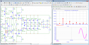
The different voltages are the output alternating (AC) voltages on the load.
There is no problem that MOS transistors can be used at any permissible voltage.
But always the result will be worse compared to BJT.
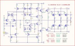
BUZ900/901 are Lateral MOS not Vertical MOS.The reason why I don't prefer VMOS I think is clear.
Yes, you're right, it's my mistake.BUZ900/901 are Lateral MOS not Vertical MOS.
The example is exactly with Lateral MOS precisely because things with them are the best
With ordinary MOS things will be even worse
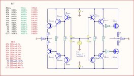
the implementation is important, in the attachment there is an option on vertical mosfets.But always the result will be worse compared to BJT.
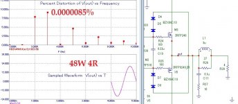
such low distortions turned out, because. applied progressive correction.
Attachments

with laterals, the practical implementation is still more complicated than it might seem in the model...The example is exactly with Lateral MOS precisely because things with them are the best
Everyone has the right to their own opinion and their own fantasies.Others may not agree with your best or worse statement.
If the opinion is technically argued, it deserves discussion.
Fantasies are already a medical problem.
Before when the maximum Ft of the final transistors was 3-4MHz it made sense from Lateral MOS.
Because simply at 50-100KHz at maximum output power with BJT transistors they just burned out.
See post #97 further in the thread.
Today with 30MHz this is no longer a problem.
And today there are even 200-300MHz final transistors true for 50V, but this is not a particular problem.
Because simply at 50-100KHz at maximum output power with BJT transistors they just burned out.
See post #97 further in the thread.
Today with 30MHz this is no longer a problem.
And today there are even 200-300MHz final transistors true for 50V, but this is not a particular problem.
Attachments

Last edited:
Of course I can't admit such nonsense.I hope you finally admitted that the inductance at the output of the amplifier is evil
Sandy, apart from THD, do you know about any other distortions? For example, have you heard what switching (Cross-Over) distortion is?
Especially considering that the 5m cable to the column has 3,3uH inductance.
The only thing that will make such inductance 1uH/4 ohm is that it will limit the amplifier band to 636KHz.
But what if there's never going to be more than 20KHz at its entrance?
In the 80's MOSFETs were new and amplifier manufacturers jumped at them. But that was completely over after a few years. It was realized that the performance of BJTs could not be achieved with FETs. FETs are completely taboo in the audio field.
the LR circuit at the output of the amplifier and the inductance of the speaker cable are not the same thing.Of course I can't admit such nonsense.
Especially considering that the 5m cable to the column has 3,3uH inductance.
yes, this is exactly what is needed to increase the stability for the capacitive nature of the load.The only thing that will make such inductance 1uH/4 ohm is that it will limit the amplifier band to 636KHz.
Are you okay with the RC circuit at the input of the amplifier? and consider it normal.
Last edited:
I don't know who exactly banned FET transistors in audio, but some copies were created exclusively for audio. Yes, there are not many such pairs, and they are on the list of the best transistors for audio amplifiers.It was realized that the performance of BJTs could not be achieved with FETs. FETs are completely taboo in the audio field.
Another thing is that FET transistors need more advanced voltage amplifiers and much more feedback depth than when using bipolar transistors. And this means that simple drivers with single-pole correction and small feedback depth are not suitable for FET transistors.
They're not the same thing, so there's got to be an RL circuit in the amplifier output.the LR circuit at the output of the amplifier and the inductance of the speaker cable are not the same thing.
But equally they won't change the sound.
The cable, in addition to inductiveness, also has the capacity unfortunately.
And precisely because of the capacity of the cable, there has to be an LR circuit in the amplifier output, and not because of the capacity in the speaker that is used there by technically illiterate people.
No one has banned MOS transistors in amplifiers.I don't know who exactly banned FET transistors in audio, but some copies were created exclusively for audio. Yes, there are not many such pairs, and they are on the list of the best transistors for audio amplifiers.
Another thing is that FET transistors need more advanced voltage amplifiers and much more feedback depth than when using bipolar transistors. And this means that simple drivers with single-pole correction and small feedback depth are not suitable for FET transistors.
It's just that apart from image, and among a certain circle of users, they don't give anything more than technical parameters
A deep feedback connection with them cannot be done because their speed is not greater than a modern BJT.
And significantly, their small gain (S) also gives a large distortion.
There are a lot of explanations here, but you have to translate.
Attachments

Last edited:
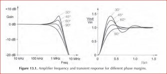
That closed loop gain peaking is in tens MHz region, importand for opamp used at that frequencies, but an audio amp can correct this peaking with LP filter at the input.That's a very good THD.
But I always look at things from another point of view: Can it be even better?
And never just look at THD.
Growth rate and PRSS are also looked at.
Things always come down to acceptable compromises between a set of parameters.
In this 100W-CFA, the small THD is the result of a two-pole frequency response.
When measuring with sine, this gives good results.
But here we do things for ourselves and not to lie to clients with parameters.
But with this type of frequency correction, the signal at the output slowly reaches 0.1-0.01% accuracy.
That's why I never use such frequency correction.
And as you can see it doesn't prevent if things are done right the THD becomes better at 2 times the output power
This peak is a function of the phase margin, and does not need to be compensated.
30-45 degrees is perfectly acceptable, and with such a phase margin, there will be deeper feedback, and hence lower THD.
But then the amplifier becomes more sensitive to capacitive loads if measures are not taken for this with an RL circuit at its output.
The input RC circuit is typically 1k/100pF (1.6MHz) to prevent radio interference from entering the input.
Attachments
- Home
- Amplifiers
- Solid State
- Apex A40 fundamental improvement. (Sandy)