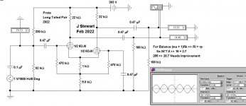
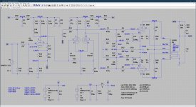
Problem solved, follow the examples. The Mullard long tailed inverter has no problem driving the output.
The 2nd sim shews your long tailed pair, looks OK driven by One Volt.
In the 3rd 2V starts to shew some clipping, not enough p-p to drive the output.
The 4th shews 2.5V, overload.
The 5th is biased up like the Mullard & easily drives the output. The balance is also a little better.
There are other ways to get here, but this works well.
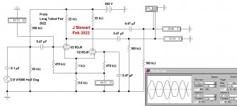
Attachments


I agree with you on the reliability of most if not all OPT models, but using a different voltage ratio between anode and screens and a different reflected impedance will change alot the behaviour of the output tubes, so at least I would put it right in the simulation. The OPT is a 4k-8 Ohm (based on the 22.3 ratio written as note).Oh wait, I should've mentioned that, don't mind the transformer values in the LTspice schematic, those are anything but accurate.
I'd suggest you to set the data based on the OPT you'll use just to give the right voltage ratio to screens and load to the output tubes:
With your current 3 to 1 ratio (15 and 5H), UL ratio is 36.6% and primary inductance 150 H, so you should have 300 mH on the 8 Ohm secondary tap.
With 100 mH on 8 Ohm on the secondary, reflected impedance is 12k.
E.G. with a primary inductance of 427 H (I've used Toroidy's value) a 40% tap will be:
L1 = L2 = 427 H x 0.2^2 = 17.08 H
L4 = L5 = 427 H x 0.3^2 = 38.43 H
L3 = 427 H x (8 / 4000) = 854 mH
Couple of other suggestions. Take a look at the driver waveforms on the grids of the output tubes. This is what the NFB is having to do to correct the distortion. Sometimes you can get HF instability which only occurs when the signals get larger. If you see this often reducing the resistor on the dominate pole (R37) helps a lot.
Thanks! I dusted off the R&S LCR bridge and took some measurements of the Ogonowski LO-PP80-1 OPT, here's what I found, these values may seem low, but take note these are at 1kHz as that's the frequency I'm using in the simulator for modelling the amplifier, so it seemed wrong to use 50Hz measurement data. Also the LCR bridge tops out at 1.5Vpp, which may not be enough to get an accurate measurement. I'm measuring the OPT without anything connected between the Anode, UL and B+ connections, so I'm measuring one half of the PP transformer.I agree with you on the reliability of most if not all OPT models, but using a different voltage ratio between anode and screens and a different reflected impedance will change alot the behaviour of the output tubes, so at least I would put it right in the simulation. The OPT is a 4k-8 Ohm (based on the 22.3 ratio written as note).
I'd suggest you to set the data based on the OPT you'll use just to give the right voltage ratio to screens and load to the output tubes:
With your current 3 to 1 ratio (15 and 5H), UL ratio is 36.6% and primary inductance 150 H, so you should have 300 mH on the 8 Ohm secondary tap.
With 100 mH on 8 Ohm on the secondary, reflected impedance is 12k.
E.G. with a primary inductance of 427 H (I've used Toroidy's value) a 40% tap will be:
L1 = L2 = 427 H x 0.2^2 = 17.08 H
L4 = L5 = 427 H x 0.3^2 = 38.43 H
L3 = 427 H x (8 / 4000) = 854 mH
Primary LO-PP80-1
Anode to UL > 1.88H > Rdc=36.3 Ohm
UL to B+ > 1.2H > Rdc=23.6 Ohm
Secondary LO-PP80-1
8 Ohm winding > 67mH > Rdc=0.5 Ohm
I also measured parasitic inductance, which is the parasitic part of the primary winding that's not coupled to the secondary. I measured parasitic inductance by shorting the secondary 8 Ohm winding leaving the 4 Ohm winding open and measured between Anode and B+ on the OPT.
Parasitic inductance
5.8mH
Since I had the tools out I also wanted to take a look at parasitic capacitance. Which I measured by shorting the Anode, UL and B+ on the primary side and the 8 Ohm winding on the secondary side individually and subsequently measuring the capacitance between these shorted primary and secondary windings.
Parasitic capacitance
3.4nF
I added these in the schematic, see attached, and ran some simulations, but I get the distinct impression this still doesn't accurately reflect reality?
Attachments
Nop the leakage inductance sets the coupling factor. The primary capacitance is just across the total primary.
Here's an example
* Model of 100PP2K2S transformer
.SUBCKT 100PP2K2S 100 102 104 106 108 204 202 200
.PARAM Lp=670 ; TOTAL PRIMARY L (FROM SPECS).
.PARAM Rp=190 ; TOTAL PRIMARY R (FROM SPECS).
.PARAM Tap=.35
.PARAM Leak=3.8e-3
.PARAM Rs=.08 ; SECONDARY R (FROM SPECS).
.PARAM Rs2=.07 ; SECONDARY R (FROM SPECS).
.PARAM Lrat={4/2200} ; INDUCTANCE RATIO: (4 OHMS)/(PRIMARY).
.PARAM Cp=345p
.PARAM QFCTR={Lp/Leak} ; Q-FACTOR
L10 100 101 {Lp*(1-Tap)(1-Tap).25}
R10 101 102 {Rp*(1-Tap)*.5}
L11 102 103 {Lp*Tap*Tap*.25}
R11 103 104 {Rp*Tap*.5}
L12 104 105 {Lp*Tap*Tap*.25}
R12 105 106 {Rp*Tap*.5}
L13 106 107 {Lp*(1-Tap)(1-Tap).25}
R13 107 108 {Rp*(1-Tap)*.5}
C10 100 108 {Cp}
L20 200 201 {Lp*Lrat}
R20 201 202 {Rs}
L21 202 203 {Lp*Lrat*1.412}
R21 203 204 {Rs2}
K1 L10 L11 L12 L13 L20 L21 {1-1/(2*QFCTR)}
.ENDS
Some of the * keep getting deleted but its obvious
Last edited:
Symbol:
Version 4
SymbolType CELL
LINE Normal -19 -160 -47 -160
LINE Normal -19 -64 -48 -64
LINE Normal -19 0 -48 0
LINE Normal -19 64 -48 64
LINE Normal -19 160 -48 160
LINE Normal -1 163 -1 -163 1
LINE Normal 1 163 1 -163 1
LINE Normal 48 48 19 48
LINE Normal 48 80 19 80
LINE Normal 48 64 19 64
ARC Normal -27 0 -10 16 -19 16 -19 0
ARC Normal -27 16 -10 32 -19 32 -19 16
ARC Normal -27 32 -10 48 -19 48 -19 32
ARC Normal -27 48 -10 64 -19 64 -19 48
ARC Normal -27 -64 -10 -48 -19 -48 -19 -64
ARC Normal -27 -48 -10 -32 -19 -32 -19 -48
ARC Normal -27 -32 -10 -16 -19 -16 -19 -32
ARC Normal -27 -16 -10 0 -19 0 -19 -16
ARC Normal -27 -80 -10 -64 -19 -64 -19 -80
ARC Normal -27 64 -10 80 -19 80 -19 64
ARC Normal 27 48 10 64 19 48 19 64
ARC Normal 27 64 10 80 19 64 19 80
ARC Normal -27 -144 -10 -128 -19 -128 -19 -144
ARC Normal -27 -128 -10 -112 -19 -112 -19 -128
ARC Normal -27 -112 -10 -96 -19 -96 -19 -112
ARC Normal -27 -96 -10 -80 -19 -80 -19 -96
ARC Normal -27 -160 -10 -144 -19 -144 -19 -160
ARC Normal -27 80 -10 96 -19 96 -19 80
ARC Normal -27 96 -10 112 -19 112 -19 96
ARC Normal -27 112 -10 128 -19 128 -19 112
ARC Normal -27 128 -10 144 -19 144 -19 128
ARC Normal -27 144 -10 160 -19 160 -19 144
WINDOW 3 16 -144 Left 2
WINDOW 0 16 -112 Left 2
SYMATTR Value 100PP2K2S
SYMATTR Prefix X
PIN -48 -160 NONE 8
PINATTR PinName Blu
PINATTR SpiceOrder 1
PIN -48 -64 NONE 8
PINATTR PinName Blu/Yel
PINATTR SpiceOrder 2
PIN -48 0 NONE 8
PINATTR PinName Red
PINATTR SpiceOrder 3
PIN -48 64 NONE 8
PINATTR PinName Brn/Yel
PINATTR SpiceOrder 4
PIN -48 160 NONE 8
PINATTR PinName Brn
PINATTR SpiceOrder 5
PIN 48 48 NONE 8
PINATTR PinName Grn/Yel
PINATTR SpiceOrder 6
PIN 48 64 NONE 8
PINATTR PinName Grn/Yel1
PINATTR SpiceOrder 7
PIN 48 80 NONE 8
PINATTR PinName Blk/Yel
PINATTR SpiceOrder 8
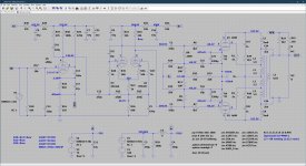
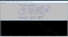
Thanks! I think I got most of it up and running, but for an odd squiggle in the gain plot. Would certainly appreciate it if you could check whether I'm not doing something monumentally stupid though. I have a pair of Hammond 1650R sitting on the shelf, so seemed logical to use that model so I can check the simulation with data from the actual prototype. Screenshot and zip archive with the latest (and greatest?) attached.If your struggling still I can look later today.
Attachments
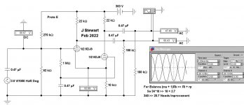
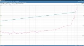
Thanks John! I tried your suggestion, but it doesn't result in a working amplifier, the lower half of the sine is compressed, resulting in distortion levels measured to be >5%. In one of my earlier prototypes I tried a similar configuration which also didn't fare too well, please see attached.Problem solved, follow the examples. The Mullard long tailed inverter has no problem driving the output.
The 2nd sim shews your long tailed pair, looks OK driven by One Volt.
In the 3rd 2V starts to shew some clipping, not enough p-p to drive the output.
The 4th shews 2.5V, overload.
The 5th is biased up like the Mullard & easily drives the output. The balance is also a little better.
There are other ways to get here, but this works well.
Attachments
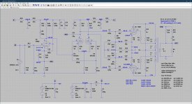
Okay John, I took another stab at it, by raising the value of the tail resistor R26 to 18K (from 10K) this results in a working amplifier, however the performance is not at the same level as the configuration I originally posted, please see attached. I think this shows that another mechanism is at play that causes for the THD to rise when Pout>20W, do you perhaps have any other suggestions?Thanks John! I tried your suggestion, but it doesn't result in a working amplifier, the lower half of the sine is compressed, resulting in distortion levels measured to be >5%. In one of my earlier prototypes I tried a similar configuration which also didn't fare too well, please see attached.
Attachments
I would have concerns taking some of the NFB to the plate of the LPT. This is because when that output valve goes out of conduction in higher power - that part of the loop will no longer have any effect so may make for HF burst on that part of the cycle. Consider taking the NFB just to the first stage.
Yeah, that makes sense, I'm just playing with compensation at this point and this was one of the ideas that proved to be effective.I would have concerns taking some of the NFB to the plate of the LPT. This is because when that output valve goes out of conduction in higher power - that part of the loop will no longer have any effect so may make for HF burst on that part of the cycle. Consider taking the NFB just to the first stage.
It’s not actually feedback from the output back to the 2nd stage plate, it’s nested feedback from the 2nd stage plate to the summing node. It’s the “tube” equivalent of taking the lead compensation from the output of the VAS rather than the speaker out. It’s a trick you can use to get higher levels of NFB before it sings - I do it this way all the time on big solid state amps with massively parallel output stages. The idea is that high frequency feedback (above audio) comes back without the phase shift through the output stage, letting you get away with low fT output transistors. The voltage ”gain” from the LTP through the output tubes and trafo is usually under unity for UL connection. Needs to be in order to work properly. It often takes experimentation to get it right. In a tube circuit, it may help you out with stability margin if your output trafo is rolling off a bit too fast for the level of NFB you want. Just another tool in the box.
Could you zip your latest offering so I can take a look. I have an interest in looking at distortion too. Cheers.
Post #50 has the latest, including your transformer model. Thanks!Could you zip your latest offering so I can take a look. I have an interest in looking at distortion too. Cheers.
Yes thats a large amount of NFB, I guess the series R C across the transformer primary is helping a lot.
To quote Bruno Putzeys: use Nfb and use lots of it … 🤣Yes thats a large amount of NFB, I guess the series R C across the transformer primary is helping a lot.
- Home
- Amplifiers
- Tubes / Valves
- KT88 PP - Dotting the Is, crossing the Ts