I have build a complete preamp ba-3. I am using it with my power amp, for months. Now i decided to build the ba-3 amp.
Do i have to take the ba-3 pcb from the preamp to put it in the same case ? And to build another preamp?
Do i have to take the ba-3 pcb from the preamp to put it in the same case ? And to build another preamp?
^ +1 if that's the goal.
well, yes
at least I understood that BA3 FE is made as standalone unit and that BA PP OS is made as buffer stage, without any FE in same case
that's at least logical, by what I've read - problem being DC offset (negative) on input of amp itself
Oracle1 -
This is what I am poorly trying to understand from you before we get to the solutions.
If you leave out the front end board in the amplifier and wire it like ZM shows, you have a BA-3 pre-amplifier and a (kind of) F4 power amplifier.
OR
You add the front-end (BA-3) boards like in this build guide to build a BA-3 amplifier.
Andy 😀 Help!
Edited order b/c ZM put one in the middle. So many helpful people.
Added one more edit... I would leave the working BA-3 pre-amplifier alone.
Last edited:
I have build a complete preamp ba-3. I am using it with my power amp, for months. Now i decided to build the ba-3 amp.
Do i have to take the ba-3 pcb from the preamp to put it in the same case ? And to build another preamp?
if you want to use your BA3 FE preamp only for that amp - it can stay that way , but you need to have it set for proper gain, as per article (OS having voltage gain of 1, so FE having full gain needed for amp's full output)
presuming that you used it with some other amp, it needed to be set for lower gain, more suited for regular amp, needing 2V or so for full power
+1
I will step aside b/c I clearly type too much.
I had asked from the beginning... full pre-amp or separating FE stage from OS stage. Full pre-amp clarified. Sorry Andy, I know what you meant, but I was pretty sure he had built the full pre.
Now what needs to be established is does Oracle1 want a BA-3 amplifier as designed or an "F4ish" amplifier? As said, I'd recommend leaving the BA-3 preamp alone, but ZMs suggestion to alter gain as needed once Oracle1's desires for the power amplifier are clarified more fully is very valid.
Someone with better translation please help. Sorry for any confusion.
+1
Sorry Andy, I know what you meant, but I was pretty sure he had built the full pre.
I thought I told you some time in 2020 never to say sorry to me, specifically never apologize for being right


If I might add, he actually has two other relevant options, a total of four good ones then.
1: Make nescessary changes iaw MZMs schematic iot drive the BA-2 OS in a separate case, in essence as an F4 sans input buffer.
2: Move the FE to the poweramp chassis, and build as in this guide.
3: Replace the BA-2 boards with F4 boards, parts can be reused, and JFETs the only «hard to find» parts.
4: Move the FE to the poweramp chassis, but include attenuator and input switch - making an integrated amplifier out of the BA-3.
It’s versatility creates both headaches and opportunities. Though with a stiff Cognac along with the job, opportunities prevail 🙂
just one reply is enough :
Amplifier unit alone- as F4, or as original/complete BA3?
explanation: F4 needing some 18Vrms at input for full output, BA3 needing some 2Vrms for full output
Amplifier unit alone- as F4, or as original/complete BA3?
explanation: F4 needing some 18Vrms at input for full output, BA3 needing some 2Vrms for full output
You guys are awesome. 
Andy... I said I'd bow out, but there is a 5th option...
Leave the working BA-3 pre-amp alone. Add the FE board (buy if necessary) to build an "actual" BA-3. It's the one I recommend, but I'm an odd duck. If you want an F4, build an F4.
Andy... I said I'd bow out, but there is a 5th option...
Leave the working BA-3 pre-amp alone. Add the FE board (buy if necessary) to build an "actual" BA-3. It's the one I recommend, but I'm an odd duck. If you want an F4, build an F4.
You guys are awesome.
Andy... I said I'd bow out, but there is a 5th option...
Leave the working BA-3 pre-amp alone. Add the FE board (buy if necessary) to build an "actual" BA-3. It's the one I recommend, but I'm an odd duck. If you want an F4, build an F4.
Maybe the best and easiest way to do it, and also flexible. But Oracle needs to ensure his BA3 pre is reduced enough in gain not to make a 60 db gain audio chain.
Oracle is your preamp stock gain or reduced in some way? Reducing value of R13 being the easiest and most obvious way.
Regards,
Andy
I would like to build a BA-3, but my transformers/PSU gives +/-51VDC. The J-fet will not survive. But can I supply the J-fets with a lover voltage and lift the Source resistors on the board for the Driver mosfets, and supply them with the +/-51VDC as for the output followers? will other parameters be affected, like gain? BIAS settings?
I would like to build a BA-3, but my transformers/PSU gives +/-51VDC. The J-fet will not survive. But can I supply the J-fets with a lover voltage and lift the Source resistors on the board for the Driver mosfets, and supply them with the +/-51VDC as for the output followers? will other parameters be affected, like gain? BIAS settings?
Don’t know about that suggestion, but I would think cascoding the JFETs is the easiest way. Beware that with such a high voltage, class A envelope will be quite small.
I don’t know how to cascode this circuit, but Mighty does. I do think, however, there will be less hassle just buying a new transformer. Maybe even cheaper too.
Regards,
Andy
I would like to build a BA-3, but my transformers/PSU gives +/-51VDC. The J-fet will not survive. But can I supply the J-fets with a lover voltage and lift the Source resistors on the board for the Driver mosfets, and supply them with the +/-51VDC as for the output followers? will other parameters be affected, like gain? BIAS settings?
short - no
TO220 mosfet modulation is referenced to rail, meaning that drain resistors of input JFets and source resistors of TO220 mosfets must be on same potential (top sides of course)
no other way than cascoding input JFets, analyzing dissipation of mosfets, same for output mosfets, rethinking heatsinking of small mosfets and big ones
first thing is - how much power you really need for your speakers and room and listening habits
if you don't need big power, buying dedicated xformers is lesser adventure than redoing everything** mentioned above
**it is easy, but only if you have mileage ..... but then, entire mental procedure is routine, and there is no need to ask anyone on forum
in any case, asking this sort of question (a priori!!!)*** is more than welcome and useful - it broadens knowledge and perspective
***better safe than sorry
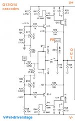
yup
that schm is informative; 2 main details are:

that schm is informative; 2 main details are:
- Pa is having shitload of TL431 and was in mood to use them ( instead of usual 2 resistors divider, even without filtration)
- Pa is taking 0V7 as Vbe; one of most important and ofte used constants in Universe
- 42 is easily divided with 0V7
- and vice versa
Thank you all, for you feedback. I guess, I need new transformers. The only other thing I can think of is series connect two of my transformers primary side, to half the secondary voltage, but that is probably not a soundwise good solution?
not good
you can use that arrangement only if there is one (summed) load at secondary side....... meaning - xformers are summed/combined both at primary and secondary
and even then - in case of parallel summing/combining on secondary side, that's best to arrange after diode bridges
- I had that brilliant idea too, eons ago, but ppl smarter than me told me reasons against
Bingo. That would be my answer, keep pre, and build a complete BA3 amp. I drove mine with a BA3 just like that. I have come to like the 2018 LS with the BA3 a little better in the system it is in.You guys are awesome.
Andy... I said I'd bow out, but there is a 5th option...
Leave the working BA-3 pre-amp alone. Add the FE board (buy if necessary) to build an "actual" BA-3. It's the one I recommend, but I'm an odd duck. If you want an F4, build an F4.
Similarly, I would also recommend BA3, odd duck status not withstanding.
Russellc
Hey, I have resumed trouble shooting this project after a hiatus and a ZenV4 build. I pretty much started over since it has been so long and I don't remember everything I have done.Pics are enlightening. Looks like you are handy with the soldering iron.
In conclusion: measurements indicate FE is OK. Do however check the following:
1: Those wires going through the riser panel holes: make sure they are fully intact. Plan to reroute or protect them better, for the long term. Those holes are quite sharp.
2: I think you allready did this, but if not make sure the front end MOSFET heatsinks are not touching anything, especially the nuts under them.
3: Let’s move on to the output stage. Starting with closeups of the boards. We need closeups of:
- bias boards
- both output stages.
- wiring to and from
- Also, please remove the big washers on your transistors, and confirm all the P channel and N channels are in the right place.
- also, confirm with DMM that there is no direct conductivity between transistor and heatsink due to metal fragments or crooked mounting. Put one probe at center pin (middle of the three solder joints on output stage), the other probe at the sink (use another CLEAN hole at the sink, so that the anodization doesn’t hinder conductivity. You want to se «OL» (over limit), or very high resistance.
- provide closeups of your zener diodes, and try to confirm correct orientation and good solder joints.
When all this is confirmed, I suggest moving along to powering up with bias levels completely turned down.
Regards,
Andy
To recap, I have a tapping/pulsing sound coming though on the outputs that is volume independent. I have gone over the FE board multiple times, replaced caps, JFETs, added an additional voltage regulation stage, and re-biased the board and am as confidant as I can be that issue is not in the FE section. I have pics of my testing on page 60 of this thread that shows results of testing that the FE board measures (via multimeter) correctly. My results today mirror those of earlier this year when I took the pics.
Multiple times I have been concerned by high DC readings on the D pins between the FE board and the OS. As before, and currently, I am getting -2.5v DC on connection D of one channel and -4.3v DC on the other channel. If I disconnect D from the FE boards then I get 0v DC on the both sides of the output caps of the FE board. As long as the OS is powered up, I will get high levels of DC on the D connections. I can zero out the offset on the speaker outs, but the tapping noise remains.
Per Andy's suggestions in the quoted post, I have visually checked every MOSFET for proper positioning and verified there was no continunity between the center pins of the MOSFETs and the heatsink. The zener's are in the correct orientation, but I have not reflowed the solder or checked the bottom of the board good solder connections. However, the solder did flow from the bottom of the board to the top and looks nice and formed properly on top. Perhaps I have bad voltage regulators on the OS?
I’d wait for a second opinion, but is this in both channels? Yes, TL431’s can be faulty, and zeners can also in some cases be noisy if defunct.Hey, I have resumed trouble shooting this project after a hiatus and a ZenV4 build. I pretty much started over since it has been so long and I don't remember everything I have done.
To recap, I have a tapping/pulsing sound coming though on the outputs that is volume independent. I have gone over the FE board multiple times, replaced caps, JFETs, added an additional voltage regulation stage, and re-biased the board and am as confidant as I can be that issue is not in the FE section. I have pics of my testing on page 60 of this thread that shows results of testing that the FE board measures (via multimeter) correctly. My results today mirror those of earlier this year when I took the pics.
Multiple times I have been concerned by high DC readings on the D pins between the FE board and the OS. As before, and currently, I am getting -2.5v DC on connection D of one channel and -4.3v DC on the other channel. If I disconnect D from the FE boards then I get 0v DC on the both sides of the output caps of the FE board. As long as the OS is powered up, I will get high levels of DC on the D connections. I can zero out the offset on the speaker outs, but the tapping noise remains.
Per Andy's suggestions in the quoted post, I have visually checked every MOSFET for proper positioning and verified there was no continunity between the center pins of the MOSFETs and the heatsink. The zener's are in the correct orientation, but I have not reflowed the solder or checked the bottom of the board good solder connections. However, the solder did flow from the bottom of the board to the top and looks nice and formed properly on top. Perhaps I have bad voltage regulators on the OS?
But if the issue is in both channels, I’d check the grounding scheme.
Did you provide pics? Can’t remember.
A quick test to provide gnd issue indications is to disconnect psu from chassis gnd and swith it on and see what happens.
- Home
- Amplifiers
- Pass Labs
- BA-3 Amplifier illustrated build guide